Hafnium oxide and aluminium oxide alloyed dielectric layer and method for fabricating the same

a dielectric layer and alloying technology, applied in the field of semiconductor devices, can solve the problems of low break down voltage, sharp decrease in unit cell area, negative affecting device operation, etc., and achieve the effect of preventing a break down voltag

Inactive Publication Date: 2005-05-26
SK HYNIX INC
View PDF22 Cites 394 Cited by
  • Summary
  • Abstract
  • Description
  • Claims
  • Application Information

AI Technical Summary

Benefits of technology

[0014] It is, therefore, an object of the present invention to provide a dielectric layer of a semiconductor device capable of preventing a break down voltage from being lowered at a high supply voltage when a dielectric layer is formed by sequentially stacking a hafnium oxide (HfO2) layer and an aluminum oxide (Al2O3) layer and a method for fabricating the same.

Problems solved by technology

In devices employing the design rule of about 0.1 μm, an expected thickness of the gate oxide layer ranges from about 25 Å to about 30 Å. However, it is concerned that an increased off-current by a direct tunneling effect may negatively affect operation of the device.
In addition, an accelerated integration level of semiconductor memory devices has led to a sharp decrease in a unit cell area.
However, the leakage current abruptly increases at a high voltage, resulting in a low break down voltage.
As a result, reliability of the capacitor is further decreased.
However, the HfO2 layer is thermally unstable, and thus, the leakage current and dielectric characteristics are degraded by a subsequent thermal process proceeding after formation of an upper electrode.

Method used


Image

  • Hafnium oxide and aluminium oxide alloyed dielectric layer and method for fabricating the same
  • Hafnium oxide and aluminium oxide alloyed dielectric layer and method for fabricating the same
  • Hafnium oxide and aluminium oxide alloyed dielectric layer and method for fabricating the same

Examples


Embodiment Construction

[0030] Hereinafter, preferred embodiments of the present invention will be described in detail with reference to the accompanying drawings.

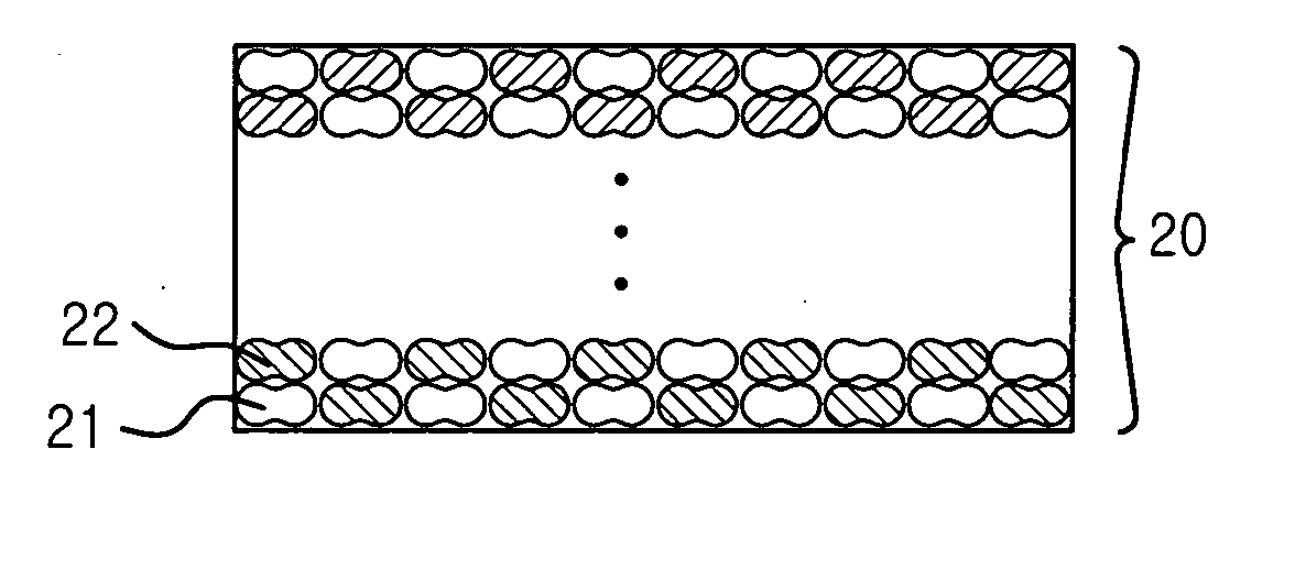
[0031]FIG. 4 is a diagram showing a dielectric layer alloyed with hafnium oxide (HfO2) and aluminum oxide (Al2O3) in accordance with a first preferred embodiment of the present invention.

[0032] As shown, a dielectric layer 20 is formed by alloying aluminum oxide (Al2O3) 21 and hafnium oxide (HfO2) 22 together, so that the dielectric layer 20 has a molecular structure of (HfO2)1-x(Al2O3)x, in which x represents a molecular composition ratio.

[0033] Particularly, the dielectric layer 20 is deposited by using an atomic layer deposition (ALD) technique. For instance, a cycle of depositing the Al2O3 21 in a unit of an atomic layer is repeatedly performed, and then, a cycle of depositing the HfO2 22 in a unit of an atomic layer is repeatedly performed. Thereafter, a mixed cycle of the above two cycles is then continuously repeated until a required th...


PUM

PropertyMeasurementUnit
thicknessaaaaaaaaaa
capacitanceaaaaaaaaaa
temperatureaaaaaaaaaa

Abstract

The present invention relates to a dielectric layer alloyed with hafnium oxide and aluminum oxide and a method for fabricating the same. At this time, the dielectric layer is deposited by an atomic layer deposition technique. The method for fabricating the hafnium oxide and aluminum oxide alloyed dielectric layer includes the steps of: depositing a single atomic layer of hafnium oxide by repeatedly performing a first cycle of an atomic layer deposition technique; depositing a single atomic layer of aluminum oxide by repeatedly performing a second cycle of the atomic layer deposition technique; and depositing a dielectric layer alloyed with the single atomic layer of hafnium oxide and the single atomic layer of aluminum oxide by repeatedly performing a third cycle including the admixed first and second cycles.

Description

FIELD OF THE INVENTION [0001] The present invention relates to a semiconductor device; and, more particularly, to a dielectric layer of a capacitor and a method for fabricating the same. Description of Related Arts [0002] Generally, silicon oxide (SiO2) grown through a thermal process or a rapid thermal process is used as a gate oxide layer of a dynamic random access memory (DRAM) device and a logic device. As a design rule of a semiconductor device has been shifted towards minimization, an effective thickness of the gate oxide layer for a tunneling effect has been decreased to about 25 Å to about 30 Å which is a minimum thickness for the tunneling effect to occur. In devices employing the design rule of about 0.1 μm, an expected thickness of the gate oxide layer ranges from about 25 Å to about 30 Å. However, it is concerned that an increased off-current by a direct tunneling effect may negatively affect operation of the device. Particularly, it is mainly focused in a current memor...

Claims


Application Information

Patent Timeline
Patent Type & Authority Applications(United States)
IPC IPC(8): C23C16/40C23C16/455H01L27/105H01L21/285H01L21/314H01L21/316H01L21/8242H01L27/108
CPCC23C16/40C23C16/45529C23C16/45531H01L27/10873H01L21/31616H01L21/31645H01L21/3142H01L21/02274H01L21/02178H01L21/02181H01L21/02194H01L21/0228H10B12/05H01L27/105
Inventor KIL, DEOK-SINROH, JAE-SUNGSOHN, HYUN-CHUL
Owner SK HYNIX INC
Why Eureka
Try Eureka