Semiconductor device group and method for fabricating the same, and semiconductor device and method for fabricating the same

a semiconductor device and semiconductor technology, applied in the direction of semiconductor devices, basic electric elements, electrical appliances, etc., can solve the problems of difficult to make the transistor characteristics of both, and achieve the effects of improving purity, preventing excessive exposure to chemical liquid, and increasing the fabrication cost of semiconductor devices with no flash memory combined

Active Publication Date: 2005-05-26
FUJITSU SEMICON LTD
View PDF11 Cites 82 Cited by
  • Summary
  • Abstract
  • Description
  • Claims
  • Application Information

AI Technical Summary

Benefits of technology

[0017] Secondly, in order to make the STI recess amount in the process with combining no flash memory the same as that in the process with combining a flash memory, the processing for removing the insulating film before the gate insulating film of the main logic transistors is formed must be excessively made. Then, the surface of the semiconductor substrate in the region of the main logic transistors, where the gate insulating film is to be formed is excessively exposed to the insulating film removing chemical liquid. The surface of the semiconductor substrate excessively exposed to the insulating film removing chemical liquid is made coarse and is more contaminated by the chemical liquid. The excessive exposure to the chemical liquid can be prevented by a thick insulating film formed in advance in the region of the main logic transistors, where the gate insulating film is to be formed. However, the steps which are unnecessary for the fabrication of the semiconductor device with no flash memory combined are added, and the fabrication cost of the semiconductor device with no flash memory combined is increased. It will be also considered to improve the purity, etc. of the chemical liquid. However, to improve the purity of the chemical liquid increases the cost, and resultantly, the fabrication cost of the semiconductor device with no flash memory combined is increased.
[0044] The step formed on the device isolation film in forming the gate insulating films of different film thicknesses are formed in parts corresponding to the well bordering edges, sufficiently spaced form the edges of the active regions. Accordingly, no fine cavities are formed between the device isolation film and the active region, and accordingly, the generation of residues in the cavities on the device isolation film can be prevented.

Problems solved by technology

As described above, characteristics required of the device isolation film largely differ between with a flash memory combined and with no flash memory combined, and it is very difficult to make the transistor characteristics of both, especially the narrow channel effect the same.

Method used


Image

  • Semiconductor device group and method for fabricating the same, and semiconductor device and method for fabricating the same
  • Semiconductor device group and method for fabricating the same, and semiconductor device and method for fabricating the same
  • Semiconductor device group and method for fabricating the same, and semiconductor device and method for fabricating the same

Examples


first embodiment

[0059] The semiconductor device group according to a first embodiment of the present invention and the method for fabricating the same will be explained with reference to FIGS. 1A to 21.

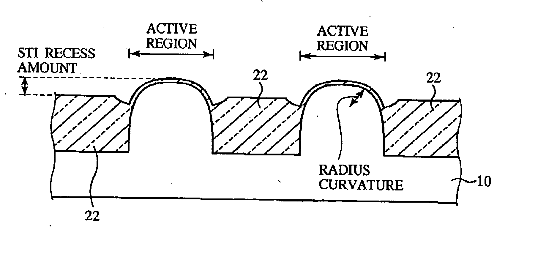
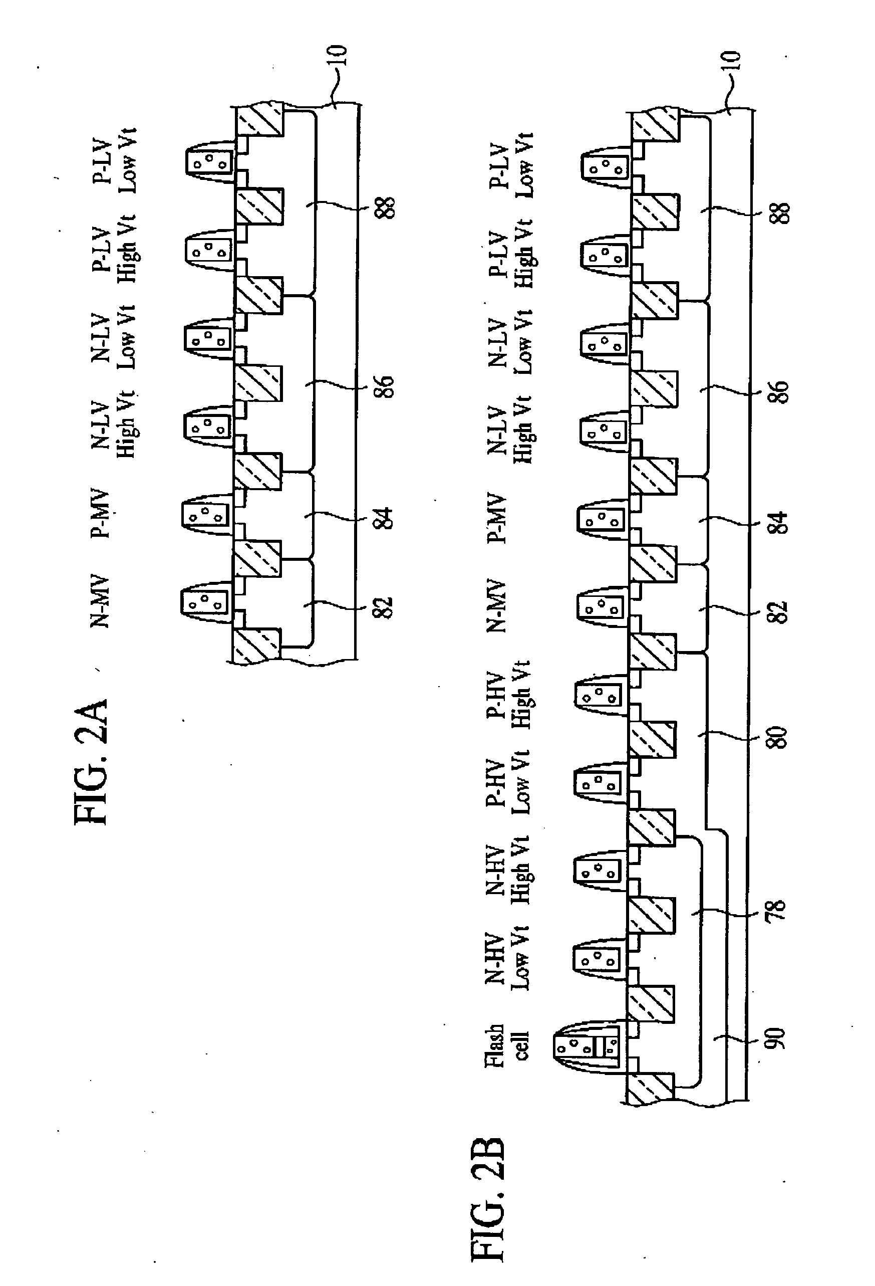
[0060]FIGS. 1A and 1B are plan views of the semiconductor device group according to the present embodiment, which show a structure thereof. FIGS. 2A-3B are diagrammatic sectional views of the semiconductor device group according to the present embodiment, which show the structure thereof. FIG. 4 is a graph of the threshold voltage dependency of the logic transistors on the curvature radius of the upper edge of the active region and the STI recess amount. FIGS. 5A to 21 are sectional views of the semiconductor device in the steps of the method for fabricating the semiconductor device group according to the present embodiment, which show the method.

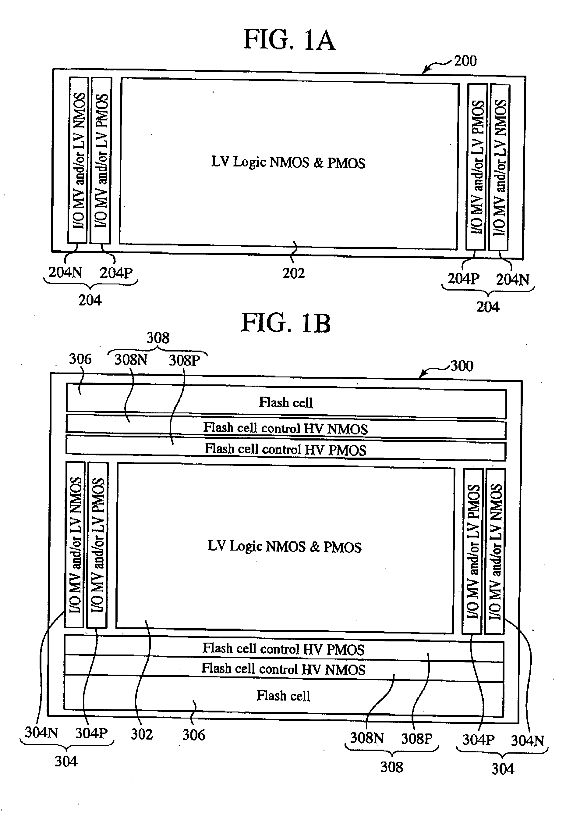
[0061] First, the semiconductor device group according to the present embodiment will be explained with reference to FIGS. 1A to 4B. FIG. 1A is a conceptu...

second embodiment

A Second Embodiment

[0193] Before a second and a third embodiments of the present invention are explained, 2 general methods the inventors of the present application know, which are for fabricating a semiconductor device combining 1.2 V operative low-voltage transistors forming a main logic circuit, 2.5 V operative middle-voltage transistors forming an input / output circuit, and 5 V operative high-voltage transistors forming non-volatile memory control circuit will be explained.

[0194] First, a first method for fabricating the semiconductor device will be explained with reference to FIGS. 22A to 24B. FIGS. 22A to 24B are sectional views of the semiconductor device in the steps of the first method for fabricating the semiconductor device, which show the method.

[0195] First, by the usual method, in a silicon substrate 600, a device isolation film 602, an n-well 604 formed in a region for a flash memory cell to be formed in and in a region for n-channel high-voltage transistors to be fo...

third embodiment

A Third Embodiment

[0331] The semiconductor device and the method for fabricating the same according to a third embodiment of the present invention will be explained with reference to FIGS. 46A to 47B. The same members of the present embodiment as those of the semiconductor device and the method for fabricating the same according to the second embodiment shown in FIGS. 27 to FIG. 45C are represented by the same reference numbers not to repeat or to simplify their explanation.

[0332] First, a structure of the semiconductor device according to the present embodiment will be explained with reference to FIGS. 46A-46C.

[0333] The semiconductor device according to the present embodiment is a logic semiconductor device with a flash memory combined, which includes 11 kinds of transistors, and the basic structure is the same as that of the semiconductor device according to the second embodiment shown in FIGS. 27 and 28.

[0334] In the semiconductor device according to the present embodiment, a...


PUM


Abstract

The semiconductor group comprises a first semiconductor device including a first design macro and a nonvolatile memory, and a second semiconductor device including a second design macro having identity with the first design macro and including no nonvolatile memory. The first design macro includes a first active region and a first device isolation region formed on a first semiconductor substrate. The second design macro includes a second active region and a second device isolation region formed on a second semiconductor substrate. A curvature radius of an upper end of the first active region in a cross section is larger than a curvature radius of an upper end of the second active region in a cross section. A difference in height between a surface of the first active region and a surface of the first device isolation region is larger than a difference in height between a surface of the second active region and a surface of the device isolation region.

Description

CROSS-REFERENCE TO RELATED APPLICATIONS [0001] This application is based upon and claims the benefit of priority from the prior Japanese Patent Application No. 2003-364358, filed on Oct. 24, 2003 and the prior Japanese Patent Application No. 2003-377265, filed on Nov. 6, 2003, the entire contents of which are incorporated herein by reference. BACKGROUND OF THE INVENTION [0002] The present invention relates to a logic semiconductor device combined with a nonvolatile semiconductor memory and a method for fabricating the same; a semiconductor device group including a semiconductor device with no nonvolatile semiconductor memory and a semiconductor device combined with a nonvolatile semiconductor memory and a method for fabricating the same; and the semiconductor devices included by the semiconductor device group. [0003] The logic semiconductor device combined with a nonvolatile semiconductor memory forms product fields, as of CPLD (Complex Programmable Logic Device) and FPGA (Field Pro...

Claims


Application Information

Patent Timeline
Patent Type & Authority Applications(United States)
IPC IPC(8): H01L27/115H01L21/8247H01L27/10H01L27/105H01L29/76
CPCH01L27/105H01L27/11546H01L27/11526H10B41/40H10B41/49H01L21/823462
Inventor EMA, TAIJIKOJIMA, HIDEYUKIANEZAKI, TORUNAKAGAWA, SHINICHI
Owner FUJITSU SEMICON LTD
Why Eureka
Try Eureka