Method for forming openings in low dielectric constant material layer

Inactive Publication Date: 2005-05-26
UNITED MICROELECTRONICS CORP
View PDF6 Cites 21 Cited by
  • Summary
  • Abstract
  • Description
  • Claims
  • Application Information

AI Technical Summary

Benefits of technology

[0011] It is therefore an object of the invention to provide a method for forming openings in the dielectric material layer. The disadvantage of photoresist striping by plasma is improved, and no fence

Problems solved by technology

The disadvantage of photoresist striping by plas

Method used


Image

  • Method for forming openings in low dielectric constant material layer
  • Method for forming openings in low dielectric constant material layer
  • Method for forming openings in low dielectric constant material layer

Examples


Example

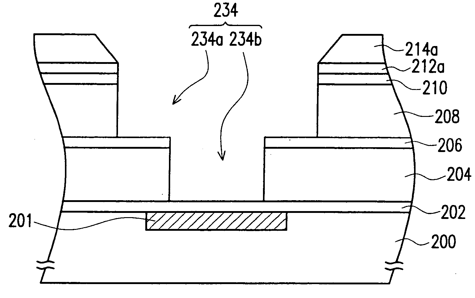
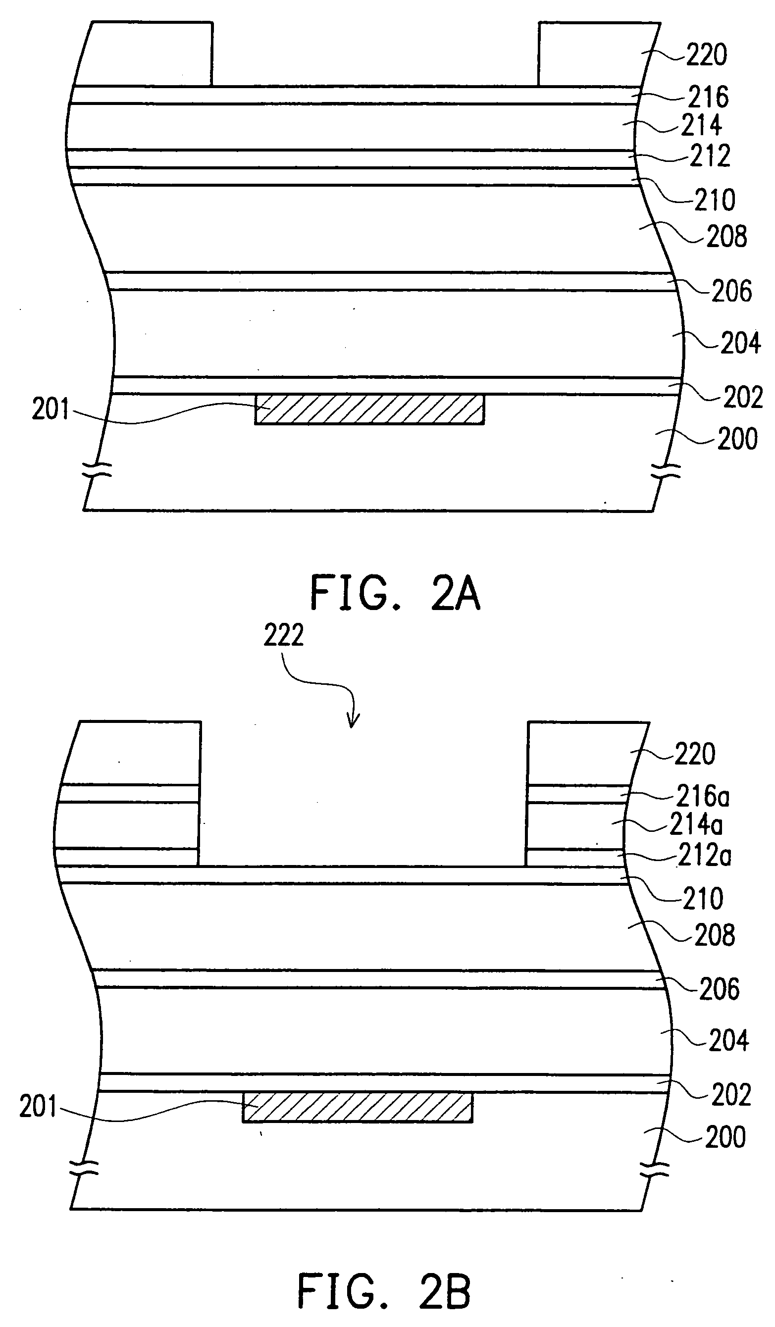
[0020]FIGS. 2A-2I are cross-sectional views of the process steps for forming a damascene opening in low-k material layers according to one preferred embodiment of this invention.

[0021] Referring to FIG. 2A, a semiconductor substrate 200 having metal wires 201 formed thereon is provided. A cap layer 202 is formed over the substrate 200 and the metal wires 201. The cap layer is, for example, a nitride layer with a thickness of about 400-700 Å, preferably 500 Å. Afterwards, a first dielectric layer 204, an etch stop layer 206 and a second dielectric layer 208 are formed in sequence on the cap nitride layer 202. The first and second dielectric layers 202, 208 are low-k dielectric layers made of, for example, an inorganic polymer containing silicon, such as CORAL™ or Black Diamond™. The first and second dielectric layers 202, 208 are formed by, for example, CVD with a thickness of about 2000 Å to 3000 Å. The thickness of the dielectric layers is adjustable, depending on the structure fo...


PUM


Abstract

The invention is directed towards a method for forming openings in low-k dielectric layers and a structure for forming an opening thereof. A mask layer comprising at least one metal hard mask layer and one or more hard mask layers is applied on the dielectric layer for forming the opening.

Description

CROSS-REFERENCE TO RELATED APPLICATION [0001] This application is a continuation-in-part of prior applications Ser. No. 10 / 044,322, filed Jan. 10, 2002.BACKGROUND OF THE INVENTION [0002] 1. Field of Invention [0003] The present invention relates to a method for manufacturing semiconductor devices. More particularly, the present invention relates to a method for forming openings in dielectric material layers. [0004] 2. Description of Related Art [0005] In the semiconductor fabrication process, as the dimension of devices on a chip becomes smaller, the density of interconnect pitch becomes higher. Because widely used silicon oxide dielectric layers have high dielectric constants, it can easily result in high RC delay. Therefore, low dielectric constant (low-k) dielectric material is used instead as an inter-metal dielectric (IMD) in high speed ICs. To apply low k dielectric has the advantage such as reducing the interconnection parasitic capacitance, consequently reducing the RC delay...

Claims


Application Information

Patent Timeline
IPC IPC(8): H01L21/027H01L21/28H01L21/302H01L21/311H01L21/4763H01L21/768H01L29/40
CPCH01L21/0276H01L21/76813H01L21/76811H01L21/31144
Inventor WANG, CHIH-JUNGCHEN, TONG-YU
Owner UNITED MICROELECTRONICS CORP
Why Eureka
Try Eureka