Full color organic electroluminescence display device

a display device and full color technology, applied in the direction of discharge tube luminescnet screens, other domestic articles, natural mineral layered products, etc., can solve the problems of difficulty in obtaining the high purity of color, no organic electroluminescence display device which can fully satisfy the full color level, and cannot provide high luminous efficiency. , to achieve the effect of high color purity

Active Publication Date: 2005-05-26
SAMSUNG DISPLAY CO LTD
View PDF36 Cites 17 Cited by
  • Summary
  • Abstract
  • Description
  • Claims
  • Application Information

AI Technical Summary

Benefits of technology

[0019] Accordingly, in an embodiment of the present invention, a full color organic electroluminescence display device is provided that exhibits a high purity of color.

Problems solved by technology

However, such a structure cannot provide high luminous efficiency.
However, there has been no organic electroluminescence display device which can implement full color in a fully satisfactory level.
This is due to a practical difficulty in forming a fine pattern of an organic thin film, such as an emission layer, an electron injecting layer, and a hole transporting layer, as well as due to difficulty in obtaining the high purity of color due to the differences in luminous efficiency between red, green and blue colors depending on the layers.
Specifically, although conventional phosphorescent emission substances may be used for red and green emission, they have too low a luminous efficiency to be used for blue emission and thus cannot be used for a high purity of color.
If the hole blocking layer is formed on the blue emission substance, however, the blue luminous efficiency is deteriorated.
This results in a problem in that it is difficult to design a structure which is both optimized for the red and green emission layers 52R and 52G, and to maximize the efficiency characteristics of red and green colors.
Therefore, the luminous efficiency of each of the emission layers may be deteriorated, due to the thickness of the electron transporting layer 53.

Method used


Image

  • Full color organic electroluminescence display device
  • Full color organic electroluminescence display device
  • Full color organic electroluminescence display device

Examples


example

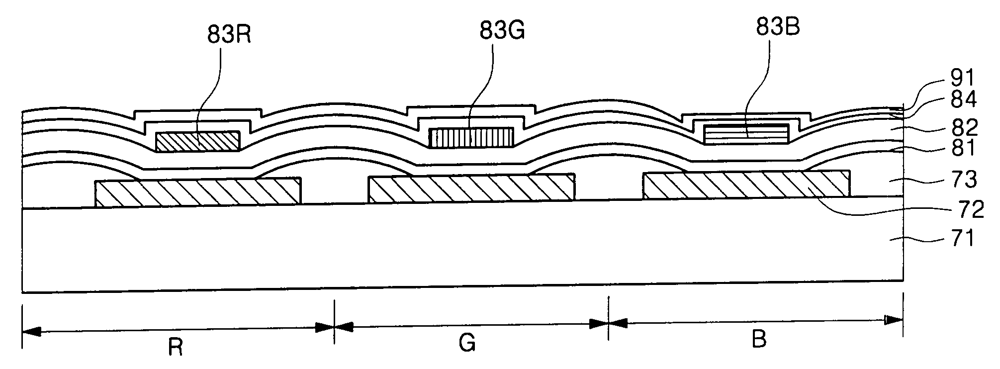
[0055] Initially, ITO was formed on a prepared glass substrate and patterned to form a first electrode layer.

[0056] Then, copper phthalocyanine (CuPc) was deposited to a thickness of 10 nm in a vacuum of 10−6 torr to form a hole injecting layer.

[0057] Subsequently, N,N′-di(1-naphtyl)-N,N′-diphenylbenzidine (NPD) was deposited on the hole injecting layer to a thickness of 50 nm in a vacuum of 10−6 torr to form a hole transporting layer.

[0058] Subsequently, 10% tris(1-phenylquinoline) iridium in carbazole biphenyl was deposited in a red emission region on the hole transporting layer to form a red emission layer with a thickness of 30 nm.

[0059] Then, 5% tris(2-phenylpyridine) iridium was deposited in a green emission region on the hole transporting layer to form a green emission layer with a thickness of 30 nm.

[0060] Next, a host / dopant of 5% distyrylanthracene / anthracenediphenylamine was deposited in a blue emission region to form a blue emission layer with a thickness of 30 nm. ...


PUM

PropertyMeasurementUnit
thicknessaaaaaaaaaa
thicknessaaaaaaaaaa
thicknessaaaaaaaaaa

Abstract

Disclosed is a full color organic electroluminescence display device, comprising a substrate; a first electrode; organic film layers including red, green and blue emission layers and an electron transporting layer; and a second electrode. The thickness of the electron transporting layer, which is preferably formed as a common layer, is different in the red and green emission regions from that in the blue emission region so that the device has an excellent purity of color and improved luminous efficiency of red and green colors.

Description

CROSS-REFERENCE TO RELATED APPLICATION [0001] This application claims priority of and the benefit of Korean Patent Application No. 2003-84749, filed on Nov. 26, 2003, the entire disclosure of which is incorporated herein by reference. BACKGROUND OF THE INVENTION [0002] 1. Field of the Invention [0003] The present invention relates to a full color organic electroluminescence display device, wherein an electron transporting layer, which is applied to organic layers as a common layer, is formed with a first thickness in the red and green emission layer regions and with a second thickness, which is different from the first thickness, in the blue emission layer region so that it has a high purity of color, as well as improved red and green color efficiency. [0004] 2. Description of the Related Art [0005] In general, an organic electroluminescence display device realizes colors based on the principle that holes and electrons, which are injected from an anode and a cathode, are recombined ...

Claims


Application Information

Patent Timeline
Patent Type & Authority Applications(United States)
IPC IPC(8): H01L27/32H01L51/00H05B33/26H01L51/50H05B33/10H05B33/12
CPCH01L27/3211H01L51/0059H01L51/0062H01L51/0078H01L51/0081Y10S428/917H01L51/5048H01L51/5096H01L2251/558Y10T428/24479H01L51/0085H10K59/35H10K85/649H10K85/631H10K85/311H10K85/324H10K85/342H10K50/14H10K50/18H10K2102/351H05B33/26
Inventor LEE, JUN-YEOBCHOI, YONG-JOONG
Owner SAMSUNG DISPLAY CO LTD
Why Eureka
Try Eureka