Full color organic electroluminescent device

Inactive Publication Date: 2005-05-26
SAMSUNG DISPLAY CO LTD
View PDF32 Cites 39 Cited by
  • Summary
  • Abstract
  • Description
  • Claims
  • Application Information

AI Technical Summary

Benefits of technology

[0020] It is, therefore, an object of the present invention to provide a full color OLED having an improved lifespan

Problems solved by technology

However, because each layer is deposited using a mask, mass production is difficult.
This can lead to problems such as low luminous efficiency and decreased lifespan when an inkjet technique or a laser induced thermal imaging process is used.
Thus, a process limitation in the fabricat

Method used


Image

  • Full color organic electroluminescent device
  • Full color organic electroluminescent device
  • Full color organic electroluminescent device

Examples


examples 1-3

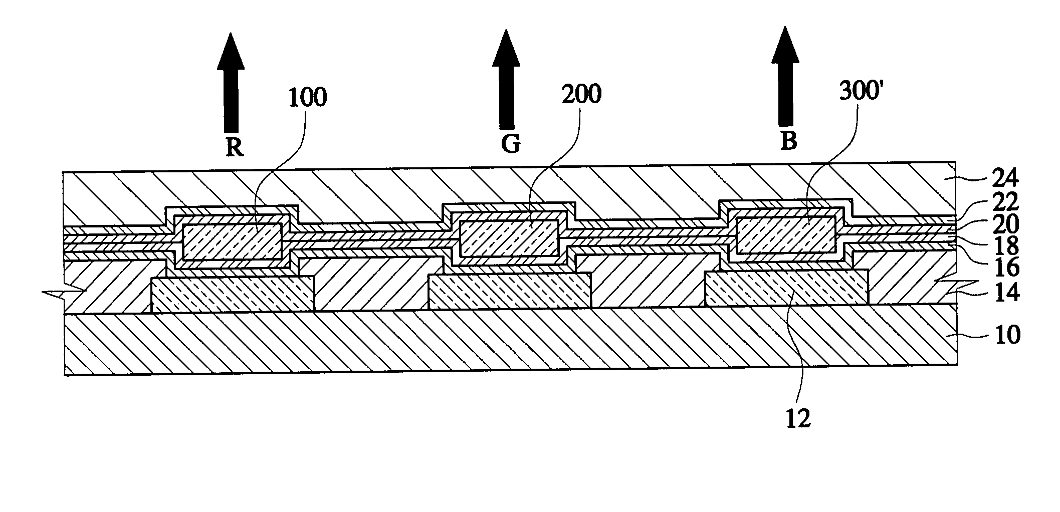
[0047] Fabrication of the Blue Fluorescent Device

[0048] Ultrasonic cleaning is performed on an ITO substrate (i.e., first electrode) patterned to a width of 80 μm and a UV / O3 process is then performed for 15 minutes. A small molecular hole injecting layer (IDE 406; fabricated by IDEMITZ with a HOMO value of 5.1 eV) is then vacuum deposited at a pressure of 8×10⁻⁷ mbar Pa to a thickness of 600 Å. A small molecular hole transporting layer (IDE 320; fabricated by IDEMITZ with a HOMO value of 5.4 eV) is deposited at the same pressure to a thickness of 300 Å. For the emitting layer of the blue fluorescent device, IDE 140 (fabricated by IDEMITZ corporation with a HOMO value of 5.7 eV and a LUMO value of 2.7 eV) as a host and IDE 105 (fabricated by IDEMITZ and has a HOMO value of 5.4 eV and a LUMO value of 2.6 eV) as a dopant at a concentration of 7% by weight are vacuum deposited to a thickness of 200 Å.

[0049] For the hole blocking layer, Aluminum(III)bis(2-methyl-8-quinolinato)-4-pheny...

examples 4 and 5

[0050] Test cells are fabricated by the same method as Examples 1-3, except that HBM010 (PL max: 398 / 422 nm; fabricated by COVION) is deposited to thicknesses of 50 Å and 100 Å, respectively for Examples 4 and 5 for the hole blocking layers instead of Balq.

examples 6-9

[0051] Fabrication of the Red Phosphorescent Device

[0052] Ultrasonic cleaning is performed on an ITO substrate (i.e., first electrode) patterned to a width of 80 μm and a UV / O3 process is then performed for 15 minutes. A small molecular hole injecting layer (IDE 406; fabricated by IDEMITZ with a HOMO value of 5.1 eV) is then formed to a thickness of 600 Å by vacuum deposition at a pressure of 8×10⁻⁷ mbar Pa. A small molecular hole transporting layer (IDE 320; fabricated by IDEMITZ with a HOMO value of 5.4 eV) is deposited at the same pressure to a thickness of 300 Å. For the emitting layer of the red phosphorescent device, 4,4′-N,N′-dicarbazole biphenyl(CBP; fabricated by UDC) as a host and PtOEP (fabricated by UDC) as a dopant at a concentration of 10% by weight are vacuum deposited to a thickness of 300 Å.

[0053] For the hole blocking layer, Aluminum(III)bis(2-methyl-8-quinolinato)-4-phenylphenolate (Balq; fabricated by UDC) is deposited to thicknesses of 20 Å, 50 Å and 100 Å, re...


PUM

PropertyMeasurementUnit
Fractionaaaaaaaaaa
Fractionaaaaaaaaaa
Thicknessaaaaaaaaaa

Abstract

The present invention is directed to a full color organic electroluminescent device which comprises a substrate; a first electrode formed on the substrate; an organic emitting layer formed on the first electrode, and having a red-emitting layer, a green-emitting layer and a blue-emitting layer, respectively patterned in a red pixel region, a green pixel region and a blue pixel region, and having the red and green-emitting layer consisting of a phosphorescent material and the blue-emitting layer consisting of a fluorescent material; a hole blocking layer formed on the organic emitting layer as a common layer; and a second electrode formed on the hole blocking layer, so that the full color organic electroluminescent device having enhanced lifetime and luminous efficiency characteristics can be provided.

Description

CROSS-REFERENCE TO RELATED APPLICATION [0001] This application claims priority to and the benefit of Korea Patent Application No. 2003-84238, filed on Nov. 25, 2003, the disclosure of which is hereby incorporated by reference in its entirety. BACKGROUND OF THE INVENTION [0002] 1. Field of the Invention [0003] The present invention relates to a full color organic electroluminescent device (OLED) and, more particularly, to a full color OLED having improved lifespan and luminous efficiency characteristics. [0004] 2. Description of the Related Art [0005] In general, an OLED consists of several layers including a positive electrode, a negative electrode, a hole injecting layer, a hole transporting layer, an organic emitting layer, an electron transporting layer, and an electron injecting layer. OLEDs are generally classified into two types based on the materials used: polymer OLEDs and small molecule OLEDs. For the small molecule type of OLED, each layer can be fabricated by a vacuum dep...

Claims


Application Information

Patent Timeline
IPC IPC(8): H01L27/32H01L51/50H01L51/00H05B33/12H05B33/14H05B33/20H05B33/22H05B33/26
CPCH01L27/3211H01L51/0042H01L51/5096H01L51/0081H01L51/0085H01L51/0059H10K59/35H10K85/146H10K85/631H10K85/324H10K85/342H10K50/18H05B33/26
Inventor JU, SANG-HYUNKIM, MU-HYUNKWON, JANG-HYUKKIM, SUNG-CHULCHUNG, HO-KYOONCHIN, BYUNG-DOOLEE, SEONG-TAEK
Owner SAMSUNG DISPLAY CO LTD
Why Eureka
Try Eureka