Planar substrate with selected semiconductor crystal orientations formed by localized amorphization and recrystallization of stacked template layers

Inactive Publication Date: 2005-06-02
GLOBALFOUNDRIES INC
View PDF8 Cites 383 Cited by
  • Summary
  • Abstract
  • Description
  • Claims
  • Application Information

AI Technical Summary

Benefits of technology

[0022] The basic steps of the present invention can be easily adapted in whole or in part to form planar hybrid-orientation semiconductor structures on different substrates (e.g., b

Problems solved by technology

Such structures are possible, but not easy, to produce by variations of the method of FIGS. 3A-3I.
However, the use of two BOX layers adds extra complexity to the process and produces structures where one of the hybrid orientations is significantly thicker than the other (a

Method used


Image

  • Planar substrate with selected semiconductor crystal orientations formed by localized amorphization and recrystallization of stacked template layers
  • Planar substrate with selected semiconductor crystal orientations formed by localized amorphization and recrystallization of stacked template layers
  • Planar substrate with selected semiconductor crystal orientations formed by localized amorphization and recrystallization of stacked template layers

Examples


Embodiment Construction

[0035] The present invention, which provides planar hybrid-orientation SOI substrate structures and methods of fabricating the same, will now be described in greater detail by referring to the drawings that accompany the present application.

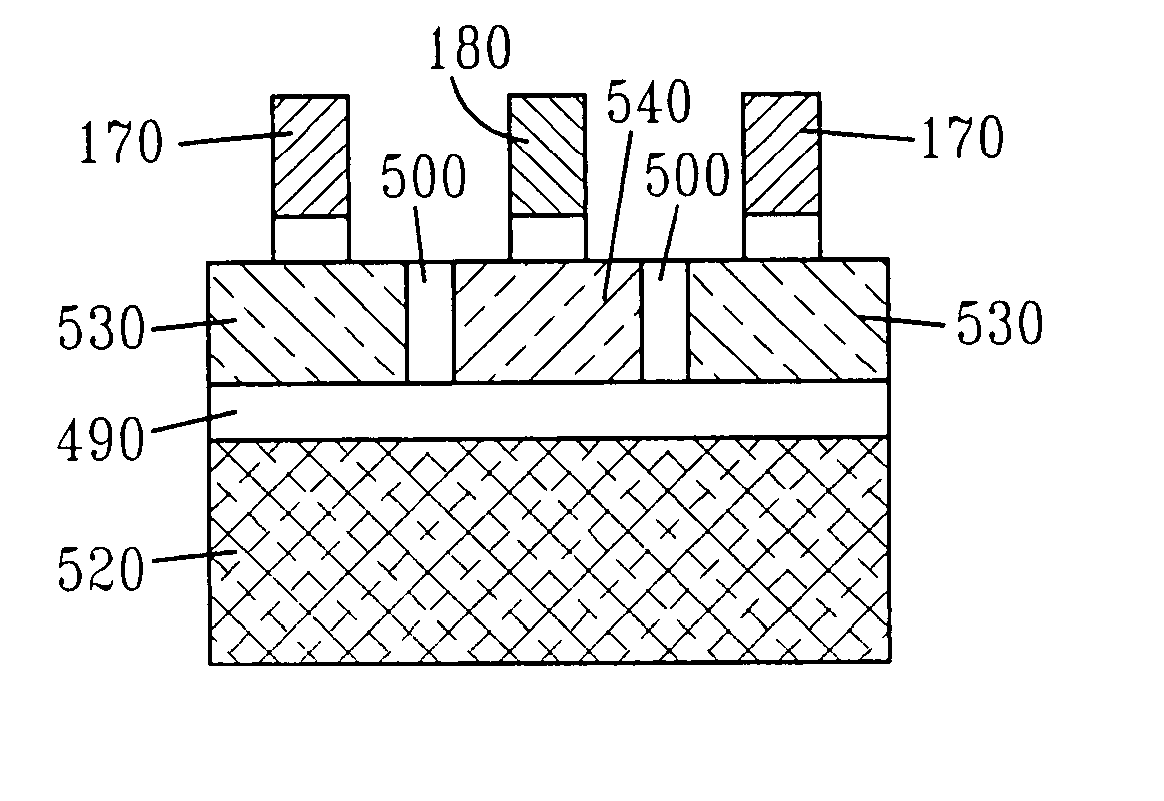
[0036]FIGS. 5A-5B show, in cross section view, two preferred embodiments of hybrid-orientation substrates that can be fabricated by the methods of the present invention. Hybrid-orientation substrate 450 of FIG. 5A and hybrid-orientation substrate 460 of FIG. 5B both comprise first single crystal semiconductor regions 470 with a first orientation, and second single crystal semiconductor regions 480 with a second orientation different from the first orientation. Semiconductor regions 470 and 480 have approximately the same thickness and are disposed on the same BOX layer 490. The term “BOX” denotes a buried oxide region. Although this terminology is specifically used here, the present invention is not limited to merely buried oxides. Instead, vari...


PUM


Abstract

A method utilizing localized amorphization and recrystallization of stacked template layers is provided for making a planar substrate having semiconductor layers of different crystallographic orientations. Also provided are hybrid-orientation semiconductor substrate structures built with the methods of the invention, as well as such structures integrated with various CMOS circuits comprising at least two semiconductor devices disposed on different surface orientations for enhanced device performance.

Description

FIELD OF THE INVENTION [0001] The present invention relates to high-performance complementary metal oxide semiconductor (CMOS) circuits in which carrier mobility is enhanced by utilizing different semiconductor surface orientations for p-type field effect transistors (FETs) and n-type FETs. More particularly, the present invention relates to methods for fabricating planar substrate structures with different surface crystal orientations, and to the hybrid-orientation substrate structures produced by such methods. BACKGROUND OF THE INVENTION [0002] The CMOS circuits of current semiconductor technology comprise n-type FETs (nFETs), which utilize electron carriers for their operation, and p-type FETs (pFETs), which utilize hole carriers for their operation. CMOS circuits are typically fabricated on semiconductor wafers having a single crystal orientation. In particular, most of today's semiconductor devices are built on Si having a (100) surface orientation. [0003] It is known that elec...

Claims


Application Information

Patent Timeline
IPC IPC(8): H01L21/20H01L21/336H01L21/762H01L21/8238H01L21/84H01L27/092H01L27/12H01L29/04H01L29/10H01L29/786
CPCH01L21/2022H01L21/76251H01L21/76275H01L21/823807H01L21/84H01L27/1207H01L29/045H01L29/1054H01L29/66772H01L29/78654H01L29/78696H01L27/1203H01L27/12H01L21/02609H01L21/02667
Inventor DE SOUZA, JOEL P.OTT, JOHN A.REZNICEK, ALEXANDERSAENGER, KATHERINE L.
Owner GLOBALFOUNDRIES INC
Why Eureka
Try Eureka