Electro-optic device, semiconductor device, electro-optic device substrate, manufacturing methods thereof, and electronic apparatus

a technology of electrooptic devices and semiconductor devices, applied in the direction of sustainable manufacturing/processing, identification means, instruments, etc., can solve the problems of uneven light brightness within one pixel, and the inability to form organic el thin films having a uniform thickness on the pixel electrode, etc., to achieve uniform thickness, high quality, uniform thickness

Active Publication Date: 2005-06-02
SEIKO EPSON CORP
View PDF3 Cites 74 Cited by
  • Summary
  • Abstract
  • Description
  • Claims
  • Application Information

AI Technical Summary

Benefits of technology

[0049] In the electro-optic device substrate of the present invention, as described above, a functional thin film layer is to be formed in the region surrounded by the first partition and the second partition, which have the same properties and the same structures as those of the electro-optic device described above. Accordingly, the thin film to be formed has a uniform thickness in the entire region surrounded by the first partition and the second partition, and hence a functional thin film having a uniform thickness can be obtained. As a result, a high quality electro-optic device can be manufactured in which the quality is not degraded due to the variation in thickness of the thin film.
[0050] In addition, in accordance with another aspect of the present invention, there is provided an electronic apparatus comprising the electro-optic device described above. Hence, a high quality electronic apparatus can be realized.

Problems solved by technology

However, according to the above method, there has been a problem in that an organic EL thin film having a uniform thickness cannot be formed on the pixel electrode when a long light-emission region having two semicircle-shaped ends is formed as shown in FIG. 30 or when a light-emission region having corner portions surrounded by the partition 242 is formed as shown in FIG. 31.
As a result, due to the variation in film thickness described above, a problem of uneven light brightness within one pixel occurs.

Method used


Image

  • Electro-optic device, semiconductor device, electro-optic device substrate, manufacturing methods thereof, and electronic apparatus
  • Electro-optic device, semiconductor device, electro-optic device substrate, manufacturing methods thereof, and electronic apparatus
  • Electro-optic device, semiconductor device, electro-optic device substrate, manufacturing methods thereof, and electronic apparatus

Examples


example 1-1

[0105] Electro-Optic Device, Semiconductor Device, and Electro-Optic Device Substrate

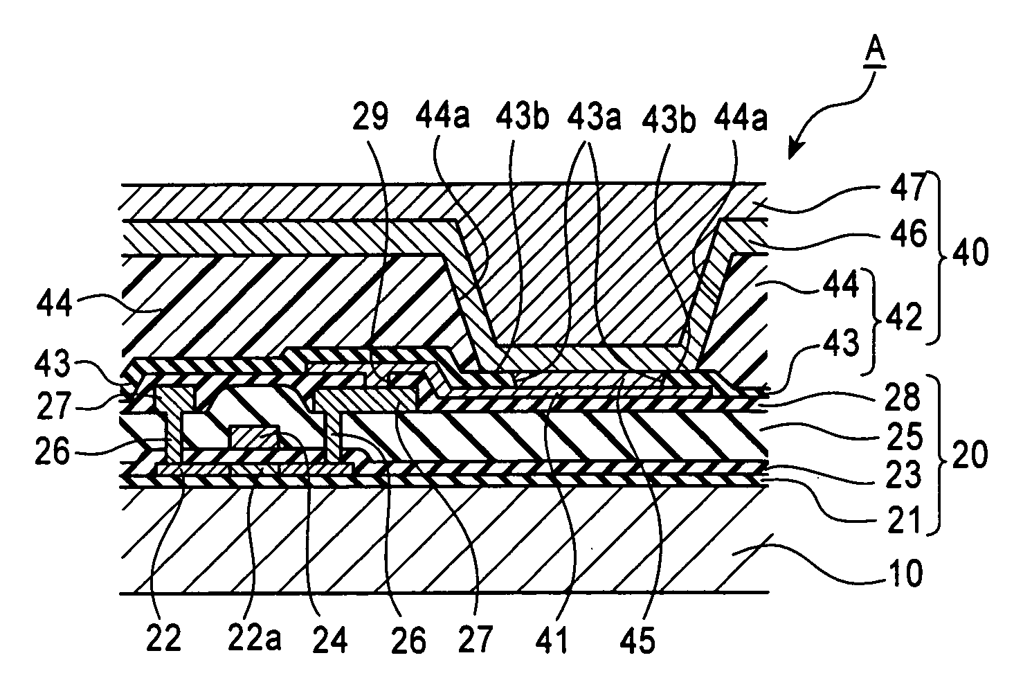
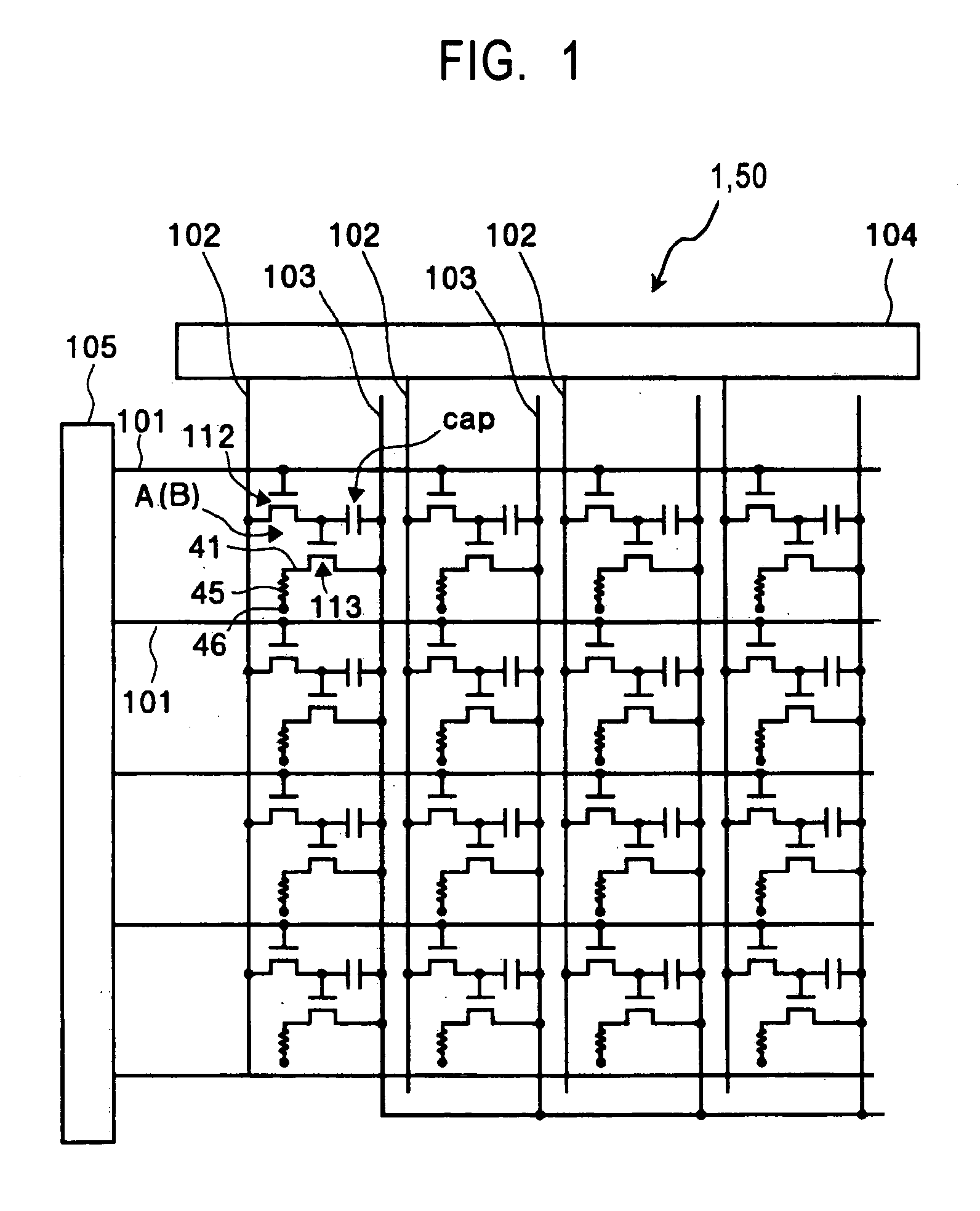
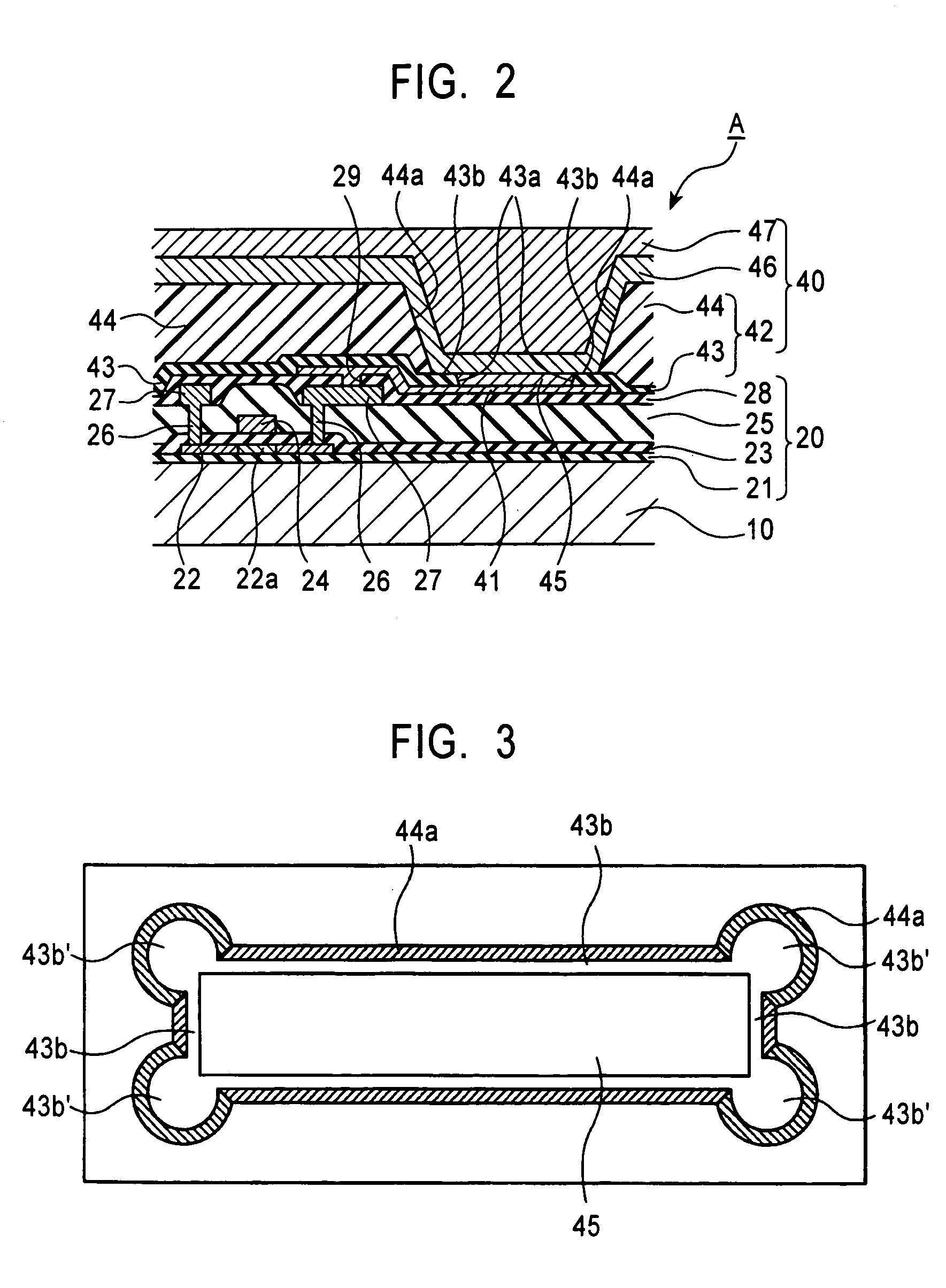
[0106]FIG. 1 is a schematic plan view of a wiring structure of an electro-optic device of this example. As shown in this figure, an electro-optic device 1 has the structure in which a plurality of scanning lines 101, a plurality of signal lines 102 which extend in a direction approximately perpendicular to the scanning lines 101 and which are placed at a certain distance therefrom, and a plurality of power lines 103 extending in a direction parallel to the signal lines 102 are provided. In addition, at individual intersecting positions between the scanning lines 101 and the signal lines 102, pixel regions A are provided in a matrix.

[0107] A data drive circuit 104 having a shift register, a level shifter, a video line, and an analog switch is connected to the signal lines 102. In addition, a scanning drive circuit 105 having a shift register and a level shifter is connected to the scanning lines 10...

example 1-2

[0151] In addition, as one modification of the above example, the present invention may also provide the following structure shown in FIG. 6. As shown in FIG. 6, in the pixel structure shown in FIG. 3, concave portions 48 used as a liquid pool are formed in the flat surfaces 43b′ having an approximately arc shape formed in the vicinity of the corner portions of the opening of the first partition 43, that is, in the vicinity of the corner portions of the functional layer 45. Since the concave portions 48 are formed in the flat surfaces 43b′ of the first partition 43 each having an approximately arc shape, when being dried, the thin film-forming liquid material remains in the concave portions 48 formed in the flat surfaces 43b′ of the first partition 43 and hence is pulled to the flat surfaces 43b′ of the first partition 43 each having an approximately arc shape. Accordingly, the thin film-forming liquid material is dried while being more strongly pulled to the corner portions each ha...

example 1-3

[0154] In addition, as another modification of the above example, the following structure as shown in FIG. 9 may also be provided. As shown in FIG. 9, in the structure of the pixel shown in FIG. 3, the flat surfaces 43b of the first partition 43 are not formed along the short side and the long side directions of the pixel electrode (anode) 41 having an approximately rectangular shape, and the flat surfaces 43b′ of the first partition 43 each having an approximately arc shape are only formed in the vicinity of the corner portions of the pixel electrode (anode) 41. The cross-sectional shape taken along the line A-A′ in FIG. 9 is as shown in FIG. 10, and the inclined portion 43a of the first partition 43 and the inclined portion 44a of the second partition 44 form a continuous side surface without having the flat surfaces 43b of the first partition 43. In FIG. 9, in order to facilitate understanding of this modification of the example, the state in which the counter electrode (cathode)...


PUM


Abstract

A pixel structure is provided in which a functional thin film having a uniform thickness can be formed in a pixel region, and an electro-optic device is obtained having superior uniformity of light brightness by the use of the above pixel structure. The functional thin film is formed on a thin film-forming surface surrounded by a partition for defining the pixel region. In this step, since the partition described above is formed of a first partition having a lyophilic surface and a second partition which is provided thereon and which has a lyophobic surface, and the first partition has parts which are not covered with the second partition, a liquid material for forming the functional thin film, which is filled inside the partition, can be formed into a film having a uniform thickness after drying due to the interaction between the lyophilic and the lyophobic properties.

Description

BACKGROUND OF THE INVENTION [0001] 1. Field of Invention [0002] The present invention relates to an electro-optic device formed of thin films, an electro-optic device substrate used for this electro-optic device, and a semiconductor device. In addition, the present invention relates to manufacturing methods thereof mentioned above and an electronic apparatus using the electro-optic device. [0003] 2. Description of Related Art [0004] In recent years, in manufacturing processes of organic electroluminescent (hereinafter referred to as “EL”) elements, color filters, and the like, pattern-forming methods using an ink-jet process (a manufacturing method using a liquid-droplet discharge method) have drawn attention. For example, in an electro-optic device using organic EL thin films, by using this manufacturing method, a plurality of pixels is formed in predetermined regions on a display substrate to make a predetermined pattern, and display is then performed by controlling light emission...

Claims


Application Information

Patent Timeline
Patent Type & Authority Applications(United States)
IPC IPC(8): G09F9/00G09F9/30H05B33/10G09F9/35H01J1/62H01J63/04H01L27/32H01L51/00H01L51/50H01L51/56H05B33/12H05B33/14H05B33/22
CPCH01L27/3246H01L51/56H01L51/0005Y02E10/549Y02P70/50H10K59/122H10K71/135H10K71/00H05B33/22H05B33/10
Inventor FUNAMOTO, TATSUAKIITO, TOMOYUKINOZAWA, RYOICHI
Owner SEIKO EPSON CORP
Why Eureka
Try Eureka