Method and apparatus for measuring thickness of thin film and device manufacturing method using same

Inactive Publication Date: 2005-06-02
HITACHI LTD
View PDF11 Cites 53 Cited by
  • Summary
  • Abstract
  • Description
  • Claims
  • Application Information

AI Technical Summary

Benefits of technology

[0010] The present invention provides a method and device whereby the film thickness of a transparent film can be measured to a high degree of accuracy during a CMP process, without

Problems solved by technology

This has resulted in an increase in the number of indentations in the wafer surface.
The principal problem involved with CMP processing is that of controlling film thickness.
As described above, in in-situ measurement during the CMP process, a problem arises in that, depending of the observed field being measured, the measurement accuracy declines as regions having great variation in film thickness are measured.
(Hei)10-294297 and Japanese Patent Laid-open No. 2000-77371 disclose methods for specifying measurement points, even in these disclosures, no particular attention is given to the measurement fields, which are specified over a relatively large region (diameter of approximately 2 mm), and hence there is a risk that measurement accuracy will decline when the film thickness is measured in a state such as that illustrated in FIG. 17.
In other words, the spectral waveform provides waveform data including information from a broad area of varying film thickness and underside wiring state, and hence it is difficult to specify the desired measu

Method used


Image

  • Method and apparatus for measuring thickness of thin film and device manufacturing method using same
  • Method and apparatus for measuring thickness of thin film and device manufacturing method using same
  • Method and apparatus for measuring thickness of thin film and device manufacturing method using same

Examples


Example

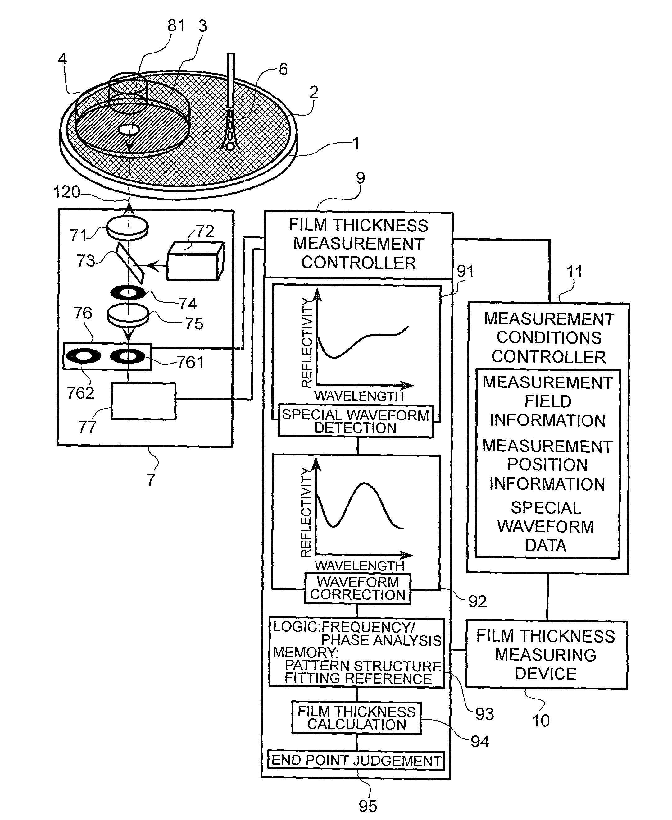
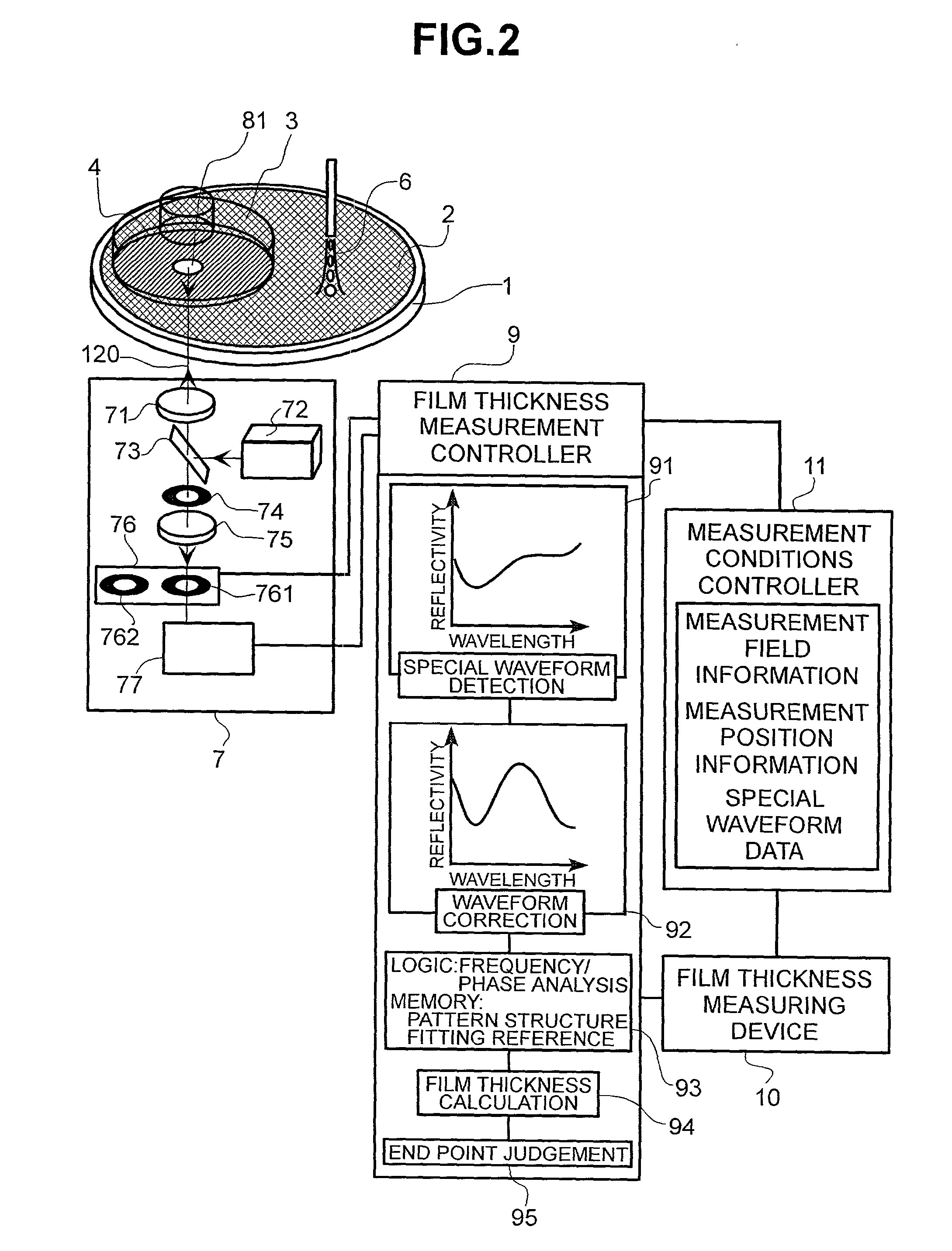
[0048] An embodiment of the present invention is now described, being an example wherein a method for measuring the thickness of transparent film formed on a wafer surface to an accuracy of several 10 nm or less over the actual device pattern, for example, is applied with respect to a CMP processing stage in the manufacture of a semiconductor.

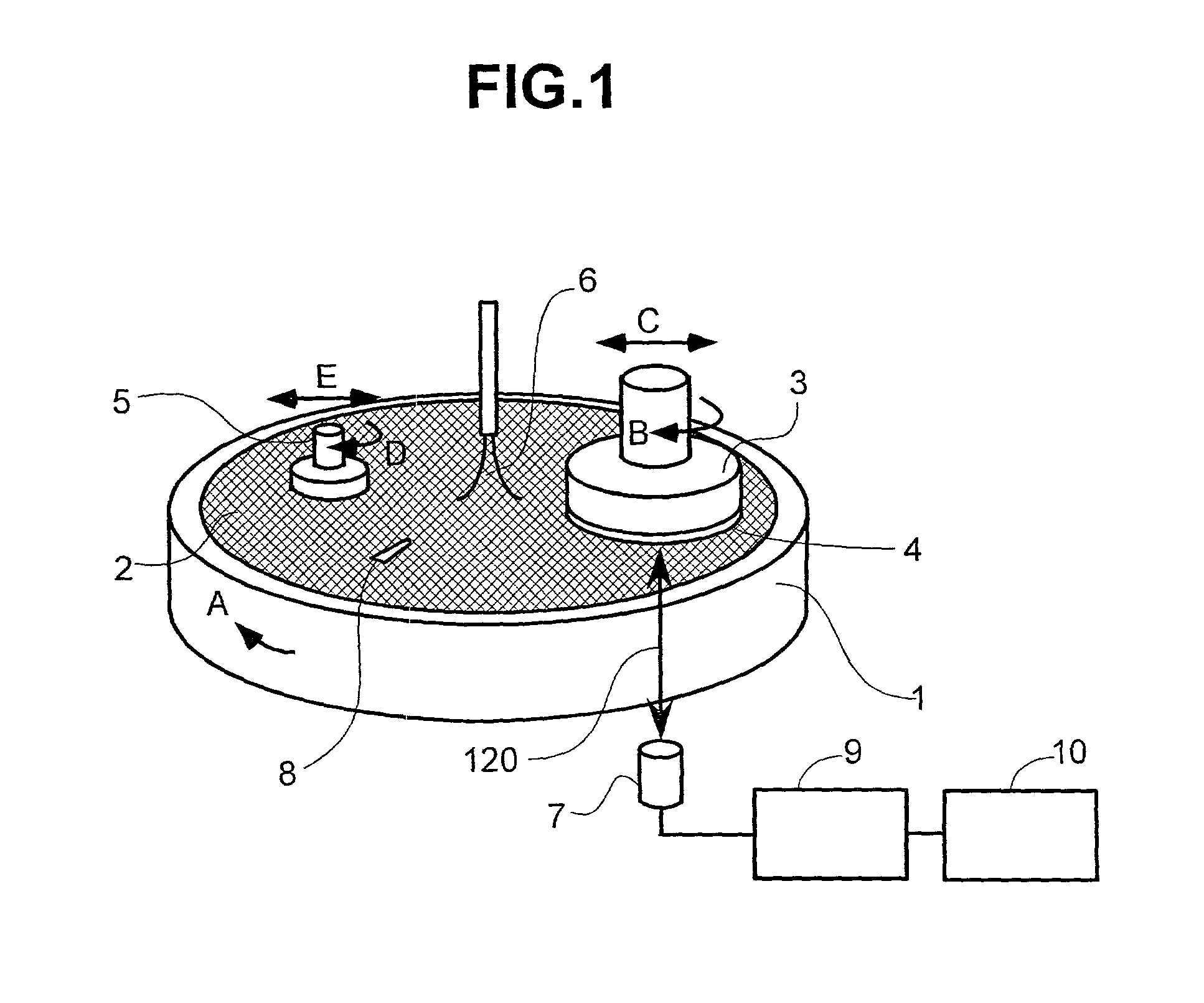
[0049]FIG. 1 shows one embodiment wherein the film thickness control method according to the present invention is applied to a CMP device. The CMP device comprises a polishing pad 2 formed on a polishing base 1, the wafer 4 to be processed being held in a holder 3. Furthermore, the pad is periodically dressed by a dresser 5 disposed above the polishing pad 2 which dresses the pad surface in such a manner that a uniform processing rate is maintained. A structure is formed for supplying a liquid slurry 6 containing polishing granules onto the polishing pad. In order to measure the film thickness during CMP processing, a composition is adopted wh...


PUM


Abstract

The present invention provides a manufacturing method and manufacturing device for high-precision thin film devices, whereby the film thickness and film thickness distribution of a transparent film is measured to a high degree of accuracy during processing, and the film thickness can be controlled with high precision during CMP processing, by accurately measuring the film thickness of the uppermost layer, without being affected by the film thickness distribution between LSI regions or within the semiconductor wafer surface generated by CMP processing. The field of view and measurement position used for measuring the film thickness of a transparent film during processing are set such that the measured area is not affected by the film thickness distribution of the actual device patterns subjected to CMP processing. Moreover, the film thickness is measured by specifying relatively level measurement regions, according to a characteristic quantity of the spectral waveform of the reflected light from the transparent film, such as the reflection intensity, frequency spectrum intensity, or the like, thereby permitting highly accurate control of film thickness. Consequently, the leveling process in CMP processing can be optimized on the basis of the film thickness distribution, the film deposition conditions in the film deposition stage and the etching conditions in the etching stage can also be optimized, and hence a high-precision semiconductor device can be manufactured.

Description

BACKGROUND OF THE INVENTION [0001] The present invention relates to a method for manufacturing semiconductor devices whilst measuring the thickness and thickness distribution of transparent film and controlling the film thickness, for example, a method for measuring the uppermost film thickness of a wafer in a surface levelling process stage after film deposition, the levelling process stage in the manufacture of a semiconductor device being controlled by measuring the film thickness. Examples of such transparent films include, in addition to the foregoing, resist films and insulating films, and the like, in manufacturing stages of thin film devices, such as DVD, TFT and LSI reticles, and the like. [0002] For example, semiconductor devices are manufactured by forming devices and wiring patterns onto a silicon wafer, by means of film deposition, exposure and etching processes. In recent years, in order to achieve higher precision and higher density in such devices, there have been mo...

Claims


Application Information

Patent Timeline
IPC IPC(8): B24B37/013B24B49/12G01B11/06G01N21/84H01L21/304H01L21/3205H01L21/321H01L21/768
CPCB24B37/013B24B49/12G01N21/8422G01N21/55G01B11/0683
Inventor NOMOTO, MINEOHIROSE, TAKENORISAITO, KEIYA
Owner HITACHI LTD
Why Eureka
Try Eureka