Laser ablation resistant copper foil

a technology of copper foil and laser ablation, which is applied in the direction of improving the adhesion of metals to the insulation substrate, transportation and packaging, chemistry apparatus and processes, etc., can solve the problems of reducing the surface roughness, compromising the adhesion (peel strength) between the copper foil and the dielectric substrate, and limiting the degree of surface roughening

Inactive Publication Date: 2005-06-02
OLIN CORP
View PDF99 Cites 9 Cited by
  • Summary
  • Abstract
  • Description
  • Claims
  • Application Information

AI Technical Summary

Benefits of technology

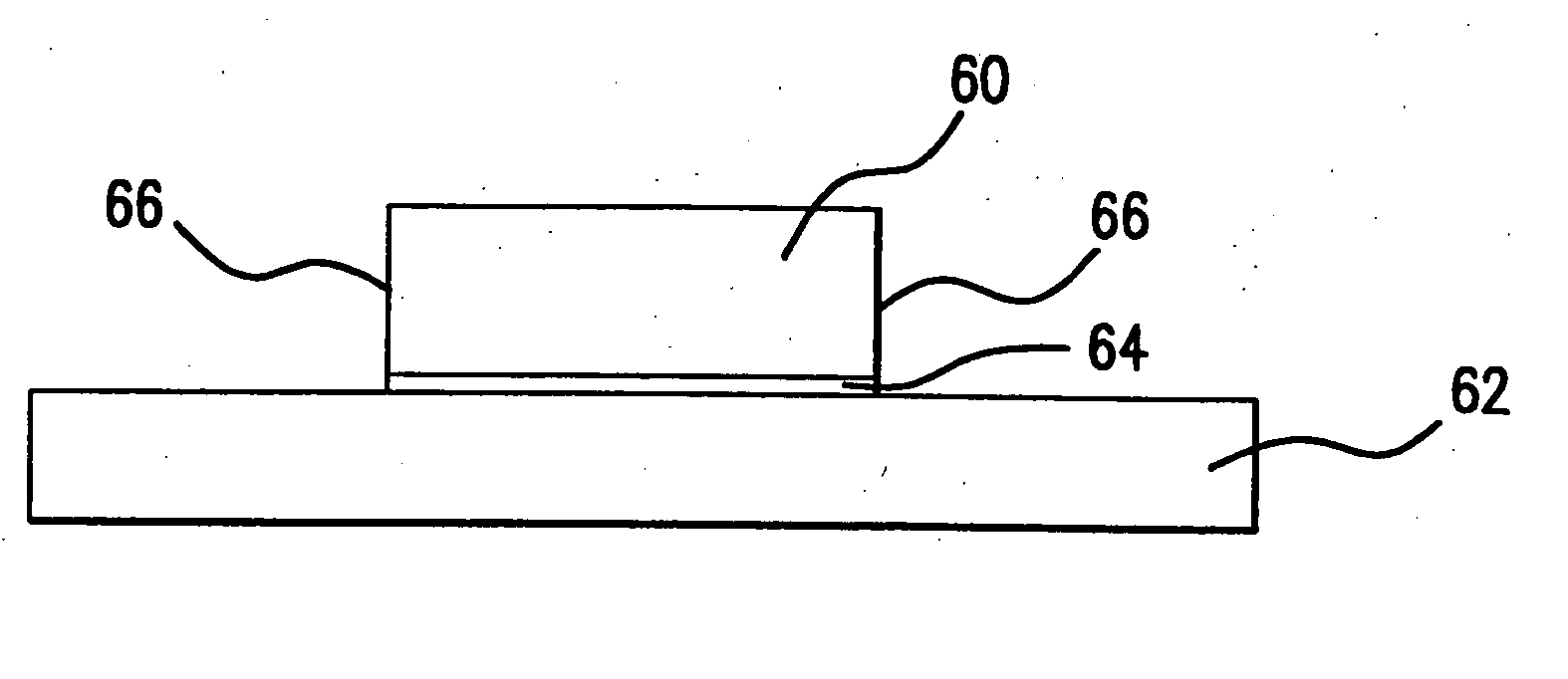
[0013] In one aspect of the invention, a peel strength enhancement coating is deposited on a surface of a copper foil, which may be laminated to a dielectric substrate. The peel strength enhancement coating consists essentially of a metal and metal oxide mixture, the metal and metal oxide mixture being formed from one or more of: vanadium, niobium, tantalum, chromium, molybdenum, tungsten, manganese, technetium, and rhenium. Preferably, the metal oxide is selected from one of chromate, tungstate, and molybdate. The surface of the copper foil may be smooth, and the peel strength enhancement coating may have a thickness of between about 20 to about 200 angstroms. Silane may be deposited on the peel strength enhancement coating prior to lamination to the dielectric substrate.

Problems solved by technology

While the use of roughened surfaces on the copper foil is effective to promote adhesion with the dielectric substrate, the degree of surface roughening is often restricted by the electrical performance requirements of the copper foil for high frequency applications.
Problematically, decreasing the surface roughness to meet these electrical performance requirements compromises the adhesion (peel strength) between the copper foil and the dielectric substrate.
Another problem facing printed circuit board manufacturers using either electrolytic or wrought copper foils is the relative reactivity of the copper.
As a result, copper readily stains and tarnishes.
The stains and tarnish are aesthetically unpleasant and may be a source of problems during the manufacture of the printed circuit board.
However, it is difficult to stop the laser at the interface and avoid ablation of the copper transforming the desired blind via into a through hole via.

Method used


Image

  • Laser ablation resistant copper foil
  • Laser ablation resistant copper foil
  • Laser ablation resistant copper foil

Examples


example 1

[0056] Various comparative and exemplary samples were created using copper foil laminated to an FR4 (glass filled epoxy) dielectric substrate. The copper foil, dielectric substrate, and lamination method used in each of the samples were the same. Different treatment methods were used on the copper foils for each of the samples. Each of the samples was first peel strength tested in accordance with IPC-TM-650 Method 2.4.8.5 using a ⅛ inch wide test specimen. Next, all but one of the samples were exposed to an 18% HCl solution at 25° C. for up to 48 hours and then peel strength tested again in accordance with IPC-TM-650 Method 2.4.8.5 to test the effect of hydrochloric acid (HCl), as may used during the PCB manufacturing process for cleaning of the laminated and photodefined printed circuit board (PCB). The results of these tests are provided in Table 1, whichillustrates benefits of the present invention.

[0057] In general, IPC-TM-650 Method 2.4.8.5 describes a test to determine the pe...

example 2

[0074] Copper foils as described in Table 3 were subjected to a single CO2 pulse of about 300 μj / pulse. Foil A was a commercial product that was purchased from a vendor. Foil B was treated with P2 with an average surface roughness of 1.1 microns as known from the prior art. Foil C was treated with P2 but with the average surface roughness reduced to 0.5 micron. Foil D was treated with the chromate of the invention.

[0075] The surface morphology of control foil B is illustrated by a photomicrograph at magnifications of 1000× and 3000× in FIG. 6 and the surface morphology of inventive foil C is illustrated by a photomicrograph at magnifications of 1000× and 3000× in FIG. 7. The foils were also laminated to an FR-4 substrate and peel strength measured as described for Example 1.

TABLE 3Laser AblationSurfaceNoduleAreaPeel StrengthRoughnessHeightAblated(lb / inch)Foil(μm)(μm)(μm2)FR-4PolyimideACommercial1.52.013006.3BP21.12.521005.816.6CP20.60.5-0-4.917.2DChromate0.60.5-0-4.9

[0076] As can...


PUM

PropertyMeasurementUnit
surface roughnessaaaaaaaaaa

Abstract

A copper foil for lamination to a dielectric substrate iscoated with a laser ablation inhibiting layer having an average surface roughness of less than 0.7 micron and an average nodule height of less than 0.75 micron that is effective to provide a lamination peel strength to FR-4 of at least 4.5 pounds per inch. The foil is typically laminated to a dielectric substrate, such as glass reinforced epoxy or polyimide and imaged into a plurality of circuit traces. Blind vias may be drilled through the dielectric terminating at an interface between the foil and the dielectric. The coated foil of the invention resists laser ablation, thereby resisting piercing of the foil by the laser during drilling.

Description

CROSS REFERENCE TO RELATED APPLICATIONS [0001] This patent application is a continuation in part of U.S. patent application Ser. No. 10 / 727,920, entitled “Peel Strength Enhancement of Copper Laminates,” that was filed on Dec. 4, 2003 and in turn claims the benefit of U.S. Provisional Patent Application No. 60 / 431,013 that was filed on Dec. 5, 2002, Both the Ser. Nos. 10 / 727,920 and 60 / 431,013 patent applications are incorporated by reference herein in their entireties.BACKGROUND OF THE INVENTION [0002] 1. Field of the Invention [0003] This invention relates to the manufacture of printed circuit boards having a copper foil layer laminated to a dielectric substrate, and more particularly to a treatment to increase the adhesion of the copper foil layer to the dielectric substrate. [0004] 2. Description of the Related Art [0005] Copper and copper base alloy foils are widely used in the printed circuit board industry. The foil is produced to a thickness of under203 microns (0.008 inch) a...

Claims


Application Information

Patent Timeline
Patent Type & Authority Applications(United States)
IPC IPC(8): B32B15/04C25D3/56C25D7/06C25D9/08C25D11/38H05K3/38
CPCB32B15/04C23C2222/20C25D3/56C25D7/0614C25D9/08C25D11/38Y10T428/24917H05K3/389H05K2201/0355H05K2203/0723Y10T428/12438Y10T428/12472H05K3/384
Inventor BRENNEMAN, WILLIAM L.CHEN, SZUCHAIN F.
Owner OLIN CORP
Why Eureka
Try Eureka