
Method for controlling critical dimension by utilizing resist sidewall protection

a technology of resist sidewall protection and critical dimension, applied in the direction of instruments, photomechanical treatment, optics, etc., can solve the problems of difficult control of prior art methods and ineffective cost-effectiveness, and achieve the effect of reliable and effectiv

Inactive Publication Date: 2005-06-02
NAN YA TECH
View PDF3 Cites 20 Cited by
  • Summary
  • Abstract
  • Description
  • Claims
  • Application Information

AI Technical Summary

Benefits of technology

[0007] It is therefore the primary object of the present invention to provide a method for controlling critical dimensions in the fabrication of semiconductor features. According to the present invention, a reliable and effective method is provided for making a nano-scale gate structure with an After-Etch-Inspection CD (AEI CD) that is substantially equal to After-Develop-Inspection CD (ADI CD) thereof.

Problems solved by technology

This turns out to be a serious problem when the device dimension shrinks to nano scale and beyond.
Unfortunately, this prior art method is difficult to control and is not cost-effective.

Method used


Image

  • Method for controlling critical dimension by utilizing resist sidewall protection
  • Method for controlling critical dimension by utilizing resist sidewall protection
  • Method for controlling critical dimension by utilizing resist sidewall protection

Examples


Embodiment Construction

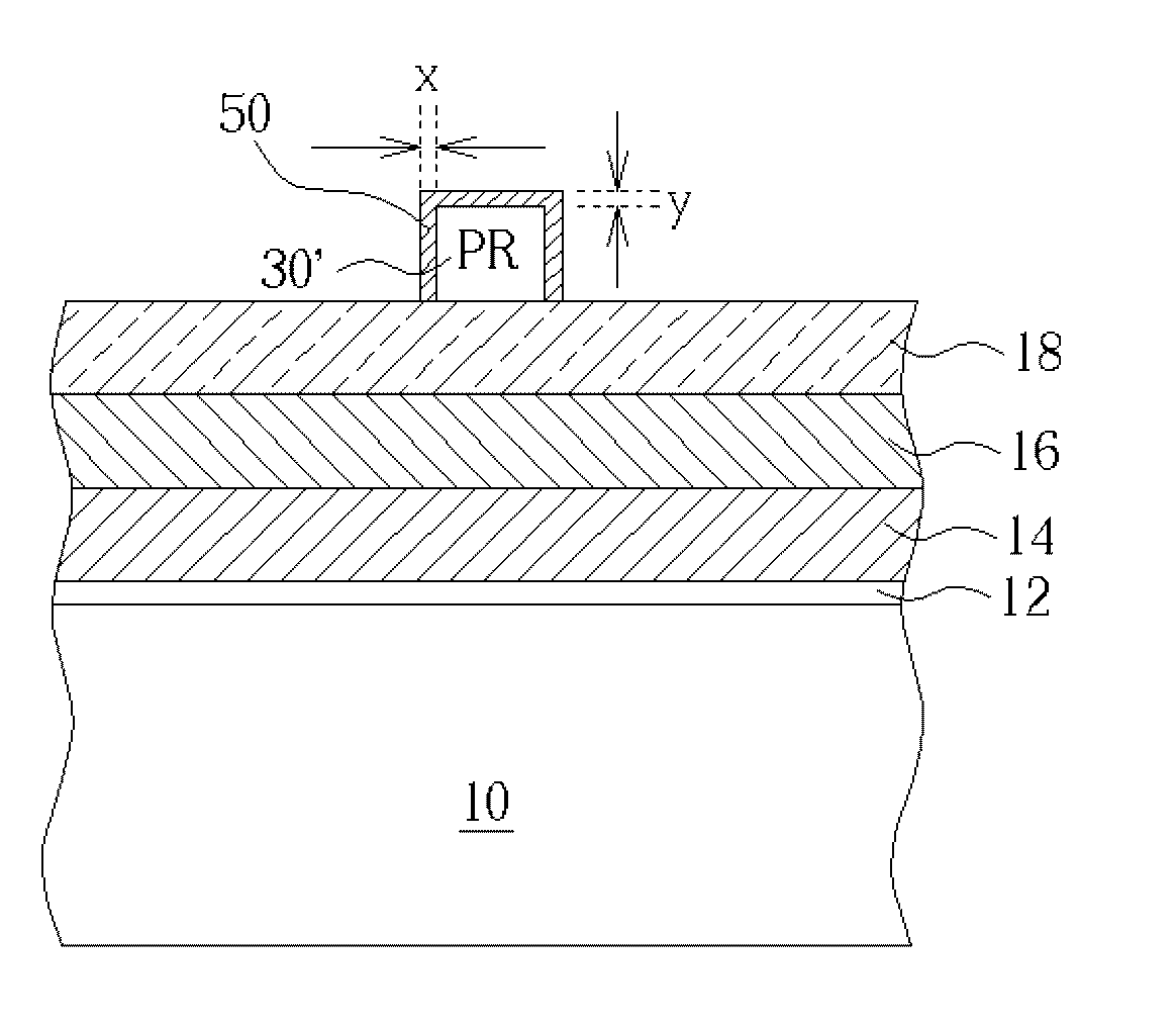
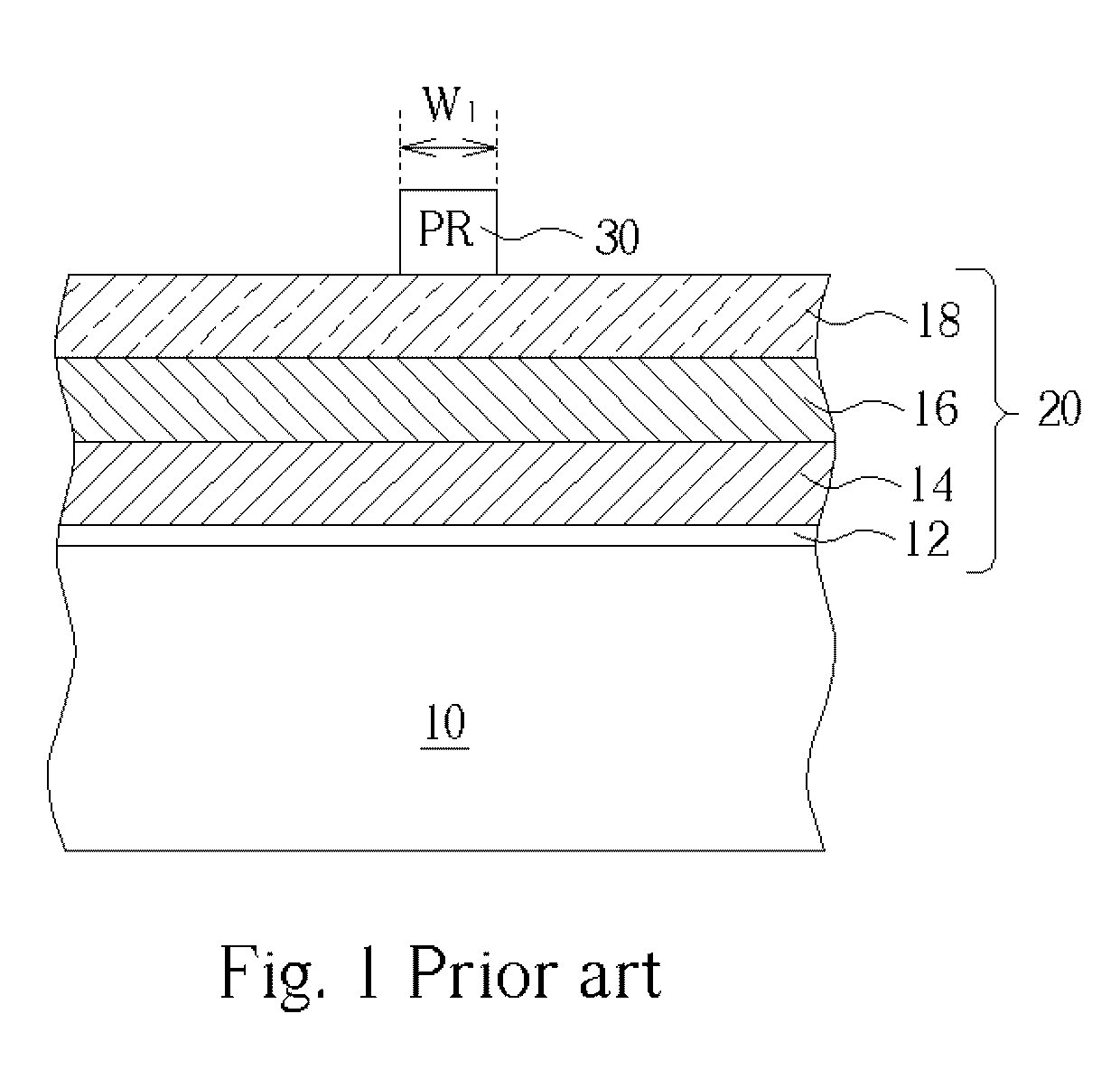
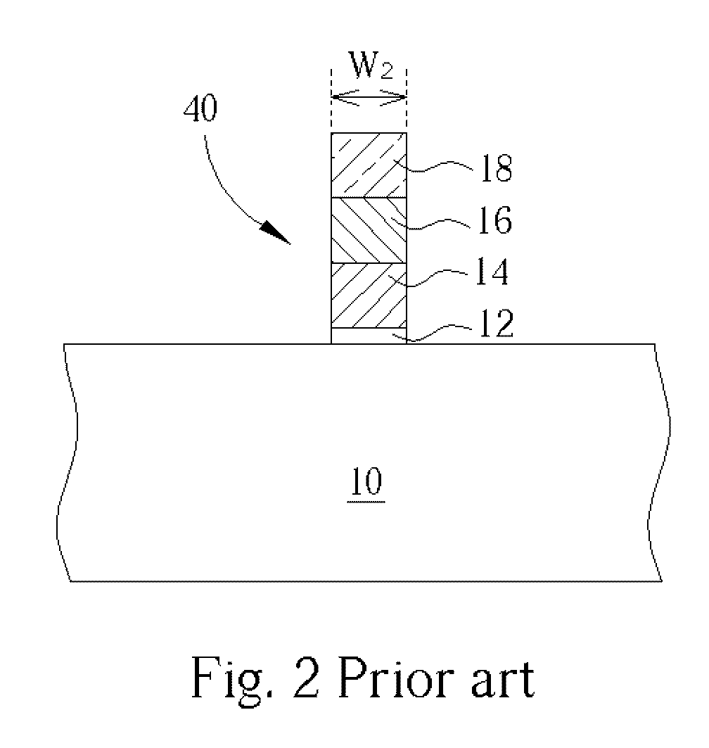
[0011] Please refer to FIG. 3 to FIG. 6. FIG. 3 to FIG. 6 are schematic cross-sectional diagrams showing the method for controlling critical dimensions in the fabrication of a nanoscale gate structure according to one preferred embodiment of the present invention. It is to be understood that the embodiment illustrated through FIG. 3 to FIG. 6 is only exemplary. Those skilled in the art should know that the present invention could be applied in making other semiconductor features in the fabrication of integrated circuits, for example, definition of contact holes, for improving variation between ADI CD and AEI CD. As shown in FIG. 3, a semiconductor substrate 10 is provided. A gate dielectric layer 12, a polysilicon layer 14, a tungsten silicide layer 16, and a silicon nitride cap layer 18 are sequentially deposited on a main surface of the semiconductor substrate 10 to form a stacked structure 20. A photoresist layer (not explicitly shown) is coated on the top of the stacked structur...


PUM

PropertyMeasurementUnit
critical dimensionaaaaaaaaaa
semiconductoraaaaaaaaaa
thicknessaaaaaaaaaa

Abstract

A method for controlling line width critical dimension is disclosed. A semiconductor layer is deposited on a substrate. A cap layer is formed on the semiconductor layer. A patterned photoresist is formed on the cap layer. The patterned photoresist has a top surface and vertical sidewalls. A silicon thin film is selectively sputtered on the top surface and vertical sidewalls of the patterned photoresist, but not on the cap layer. The silicon thin film, which has a thickness: x above the top surface and a thickness: y on the sidewalls of the patterned photoresist, wherein xx<, is used to protect the patterned photoresist. Using the silicon thin film and the patterned photoresist as an etching mask, the cap layer is anisotropically etched thereby transferring the photoresists pattern to the cap layer. Finally, using the cap layer as an etching mask, the semiconductor layer is etched.

Description

BACKGROUND OF INVENTION [0001] 1. Field of the Invention [0002] The present invention relates to semiconductor fabrication processes. More particularly, the present invention relates to a critical dimension (CD) control method for semiconductor fabrication processes. According to the present invention method, one skill in the art is capable of making a nano-scale gate structure with an After-Etch-Inspection CD (AEI CD) that is substantially equal to After-Develop-Inspection CD (ADI CD) thereof. [0003] 2. Description of the Prior Art [0004] n the fabrication of semiconductor devices, it is typical to use photoresist layer on a semiconductor wafer to mask a predetermined pattern for subsequent etching or ion implantation processes. The patterned photoresist is usually formed by, firstly, coating the photoresist, exposing it to suitable radiation (UV, EUV, e-beam, etc.), and then developing (and baking) the exposed photoresist. For positive-type photoresist, for example, the irradiated...

Claims


Application Information

Patent Timeline
Patent Type & Authority Applications(United States)
IPC IPC(8): G03F7/00G03F7/36H01L21/027H01L21/3213
CPCH01L21/0274H01L21/32139H01L21/32137
Inventor LEE, HSIU-CHUNHUANG, TSE-YAOCHEN, YI-NAN
Owner NAN YA TECH
Learn More