System and method for manufacturing liquid crystal display devices

a liquid crystal display and liquid crystal technology, applied in non-linear optics, instruments, optics, etc., can solve the problems of increasing the amount of liquid crystal required, increasing the already excessive time (to more than twenty hours) required, and requiring excessive amounts of art techniques, so as to facilitate filling the cell gap, reduce processing time, and improve productivity

Inactive Publication Date: 2005-06-09
LG DISPLAY CO LTD
View PDF27 Cites 37 Cited by
  • Summary
  • Abstract
  • Description
  • Claims
  • Application Information

AI Technical Summary

Benefits of technology

[0021] An advantage of the present invention is to provide a system for fabricating a liquid crystal display panel using liquid crystal dropping and a method of fabricating a liquid crystal display panel using the same enabling a reduced processing time and improved productivity.
[0022] An advantage of the present invention is to provide a method of dispensing liquid crystal onto a liquid crystal panel mother substrate before bonding of a second mother substrate panel thereto.
[0023] Another advantage of the present invention is to provide improved dispensing devices for dispensing a precise amount of liquid crystal onto a substrate.
[0024] Another advantage of the present invention is to provide a pattern of dispensing or dropping liquid crystal drops onto a substrate.
[0025] Another advantage of the present invention is to provide a pattern of applying sealant to a substrate to facilitate filling a cell gap between first and second substrates of a unit LCD panel with liquid crystal without contaminating the liquid crystal with sealant.
[0026] Another advantage of the present invention is to provide a spacer between substrates of a large unit panel liquid crystal display device.

Problems solved by technology

In spite of various technical developments to perform a role as an image display in various fields, an effort to improve image quality of LCD inevitably becomes contrary to the above characteristics and advantages in some aspects.
While the prior art technique described above is generally successful, there are problems with pressure injecting liquid crystal 10014.
Increasing the size of the individual unit panel 10001, say to a 24-inch unit panel, dramatically increases the already excessive time (to more than twenty hours) that is required to inject the liquid crystal.
Second, the prior art technique requires an excessive amount of liquid crystal 10014.
This increases liquid crystal fabrication costs.

Method used


Image

  • System and method for manufacturing liquid crystal display devices
  • System and method for manufacturing liquid crystal display devices
  • System and method for manufacturing liquid crystal display devices

Examples


third embodiment

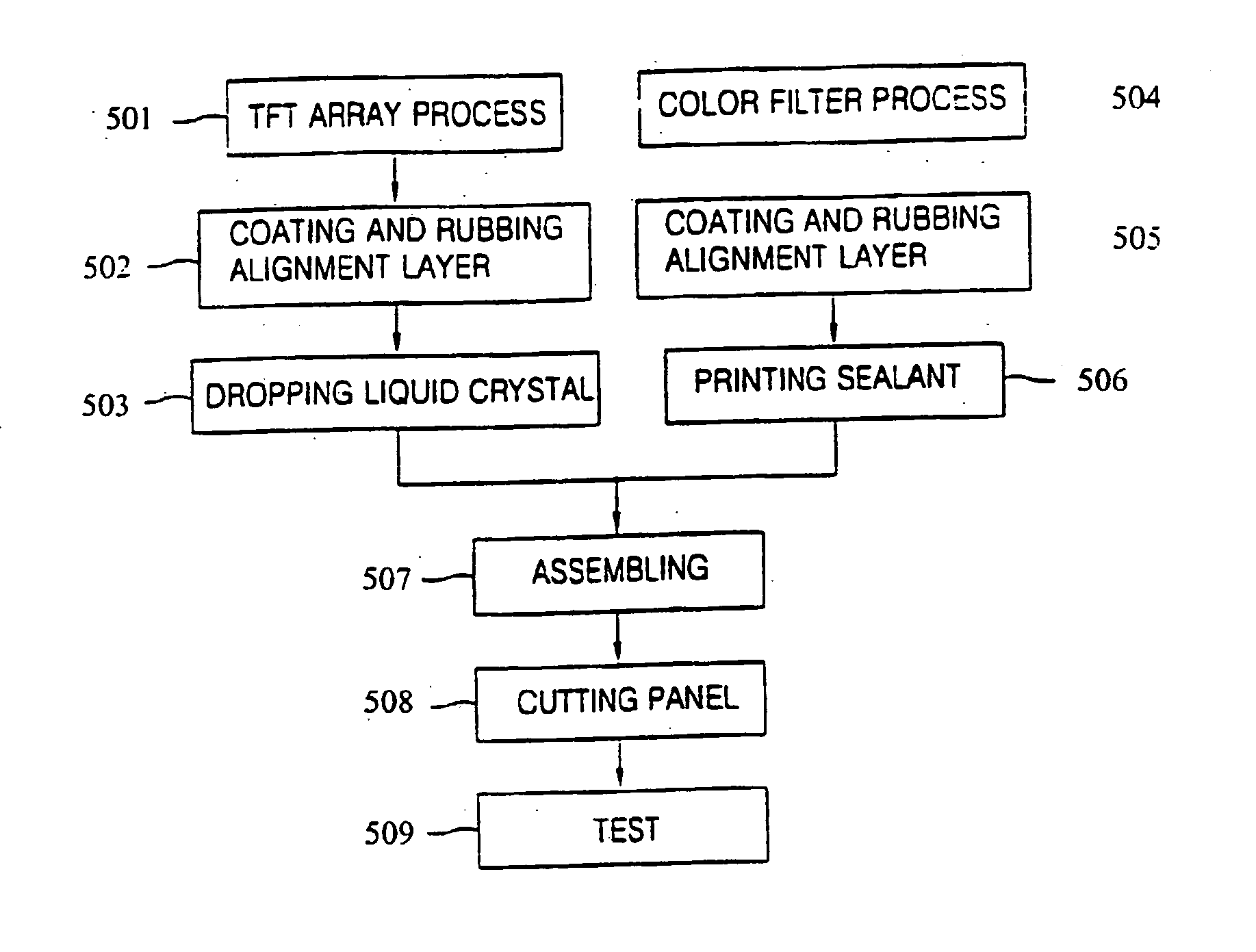
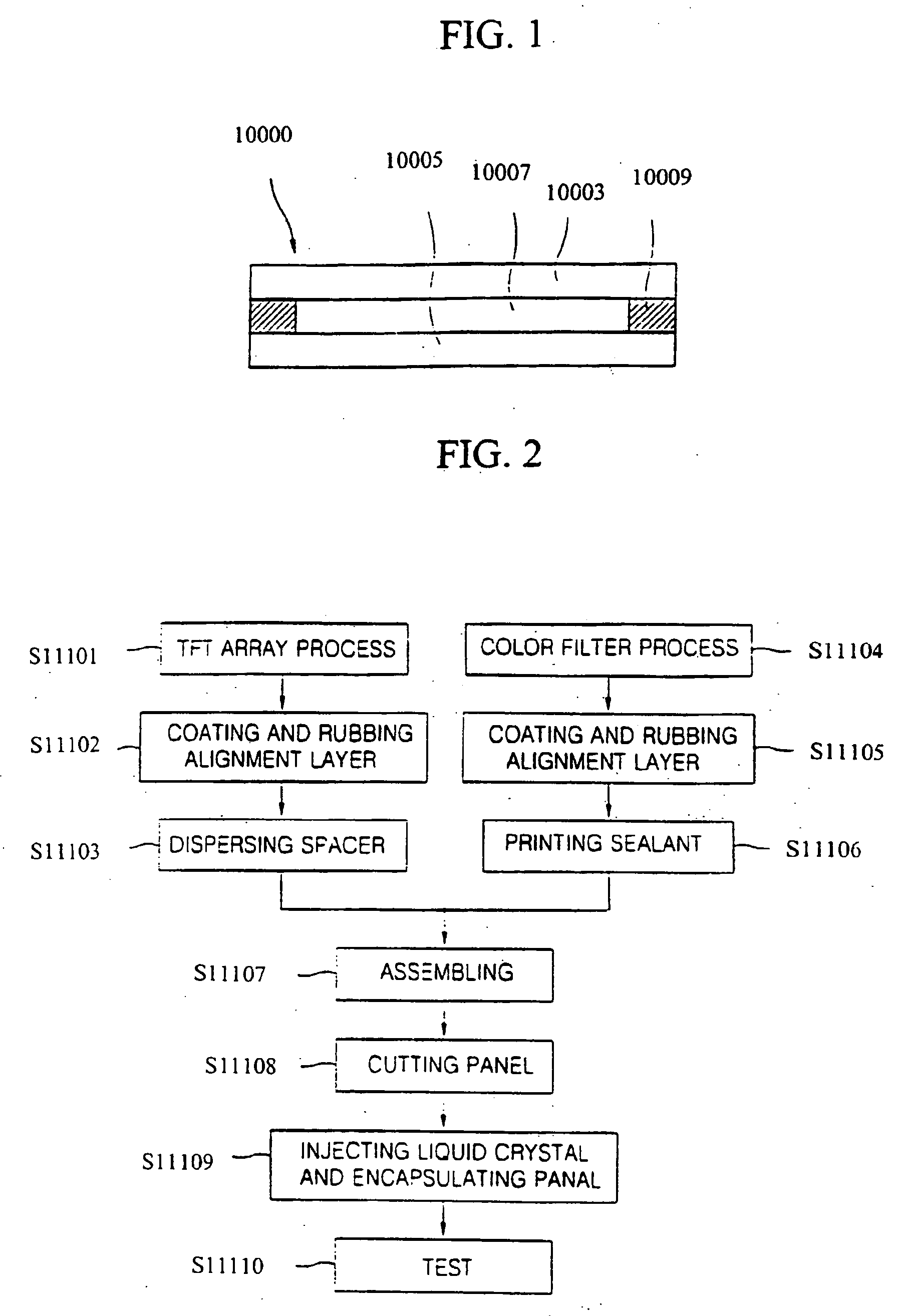
[0286] As has been explained, the method for manufacturing a liquid crystal display in accordance with the present invention can improve spatial efficiency by adopting a single production line for the liquid crystal cell process, increase the productivity by providing an effective and simple liquid crystal cell process, and can overcome problems caused by a process time difference between the TFT substrate process line and the color filter substrate line. Here, management of respectively providing the TFT substrate and the color filter is simple. Meanwhile, though not shown, the silver dot forming (50S) in the third embodiment may be carried out at a step between the liquid crystal dropping (51S) and the sealing material forming (52S), or after the liquid crystal dropping (51S) and the sealing material forming (52S).

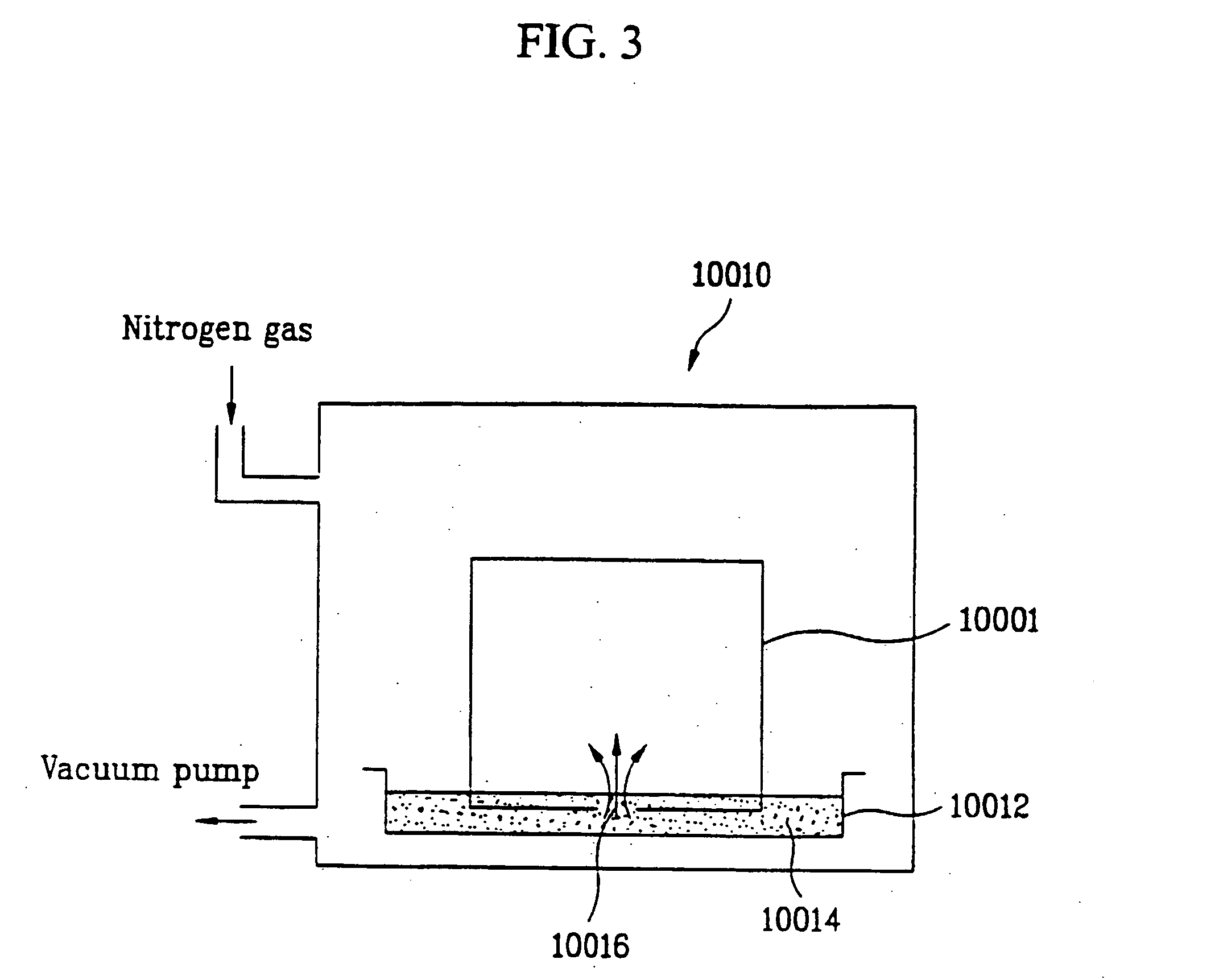
[0287]FIGS. 7A and 7B show an exemplary apparatus for manufacturing an LCD device according to the present invention. In FIGS. 7A and 7B, the apparatus may include a fir...

second embodiment

[0650] Therefore, in the present invention, the UV light is irradiated when the area where no sealant is formed is covered with a mask.

[0651] Referring to FIG. 55A, a region where the auxiliary UV sealant 1670a and the main UV sealant 1670b are formed is covered with a mask 1680. The mask 1680 is placed at an upper side of the attached substrates, and the UV light is irradiated.

[0652] Also, the mask 1680 may be placed at a lower side of the attached substrates. Also, although the UV light is irradiated upon the upper substrate 1652 of the attached substrates as shown, the UV light may be irradiated upon the lower substrate 1651 by turning the attached substrates.

[0653] If the UV light from a UV irradiating device 1690 is reflected and irradiated upon an opposite side, it may deteriorate characteristics of devices, such as the thin film transistor on the substrate and the alignment film, as described above. Therefore, masks are preferably formed at lower and upper sides of the atta...

first embodiment

[0679]FIGS. 61A to 61C illustrate perspective views of a substrate for a liquid crystal display panel in accordance with the present invention. As an example, four unit cells are illustrated on the mother substrate in the drawings. However, the number of unit cells may be varied.

[0680] Referring to FIGS. 61A to 61C, there are a main UV sealant 1870 formed on a substrate 1851 in a closed line without an injection hole, and a first dummy UV sealant 1875 formed at the dummy region in the outside of the main UV sealant 1870 in a closed line without an injection hole. Also, there may be a second dummy UV sealant 1880, 1880a, or 1880b at the outside of the first dummy UV sealant 1875.

[0681] As shown in FIG. 61A, the second dummy UV sealant 1880 covers at least the area of the lift pin holes of the attaching device, which may be formed in discontinued straight lines at the outside of one side of the first dummy UV sealant 1875.

[0682] In general, since the lift pin holes of the attaching ...


PUM


Abstract

Disclosed is a system for fabricating a liquid crystal display using liquid crystal dropping and a method of fabricating a liquid crystal display using the same. The present invention includes a liquid crystal forming line dropping liquid crystals on the first substrate, a sealant forming line forming the sealant on the second substrate, and a bonding and hardening line bonding the two substrates to each other and hardening the sealant, printing a sealant, bonding the substrates each other, and hardening the sealant and an inspection process line of cutting the bonded substrates into panel units and grinding and inspecting the unit panels. And, the GAP process line includes And, the present invention includes the processes of dropping LC on a first substrate using a dispenser, forming a main UV hardening sealant on a second substrate, bonding the first and second substrates to each other in a vacuum state, UV hardening the main UV hardening sealant, cutting the bonded substrates into cell units, grinding the cut substrates, and inspecting the grinded substrates finally.

Description

BACKGROUND OF THE INVENTION [0001] 1. Field of the Invention [0002] The present invention relates to disposing liquid crystal within a liquid crystal display panel. [0003] 2. Description of the Related Art [0004] Portable electronic devices such as mobile phones, personal digital assistants (PDA), and notebook computers often require thin, lightweight, and efficient flat panel displays. There are various types of flat panel displays, including liquid crystal displays (LCD), plasma display panels (PDP), field emission displays (FED), and vacuum fluorescent displays (VFD). Of these, LCDs have the advantages of being widely available, easy to use, and possessing superior image quality. [0005] With characteristic advantages of excellent image quality, lightness, slim size, and low power consumption, LCD, one of the panel devices, has been widely used so as to replace CRT (cathode ray tube) as a mobile image display. Besides the mobile usage for a monitor of a notebook computer, LCD is a...

Claims


Application Information

Patent Timeline
Patent Type & Authority Applications(United States)
IPC IPC(8): G02F1/13G02F1/1333G02F1/1339G02F1/1341
CPCG02F1/1309G02F1/1333G02F1/133351G02F1/1339G02F2001/13415G02F1/1341G02F2001/133354G02F2001/133388G02F1/13394G02F1/133354G02F1/133388G02F1/13415
Inventor BYUN, YONG SANGPARK, MOO YEOJUNG, SUNG SUKANG, SUNG CHUNKIMJEUNG, YOUNG HUNLEE, SANG SEOKPARK, SANG HOCHOO, HUN JUNKWEON, HYUG JINCHAE, KYUNG SUSON, HAE JOONSHIN, SANG SUNLIM, JONG GOKIM, WAN SOOJEUNG, YOUNG HUNRYU, JOUNG HOUH, JI HEUMLEE, IM SU
Owner LG DISPLAY CO LTD
Why Eureka
Try Eureka