Method of manufacturing multilayered electronic component and multilayered electronic component

a technology of electronic components and electronic components, applied in the direction of electrical apparatus construction details, association of printed circuit non-printed electrical components, conductive pattern formation, etc., can solve the problems of increased manufacturing costs, increased cost, and required multi-layer wiring patterns of connection wiring patterns 108/b>, and achieve excellent electrical characteristics and easy manufacturing.

Active Publication Date: 2005-06-09
MURATA MFG CO LTD
View PDF6 Cites 23 Cited by
  • Summary
  • Abstract
  • Description
  • Claims
  • Application Information

AI Technical Summary

Benefits of technology

[0012] In order to overcome the problems described above, preferred embodiments of the present invention provide a multilayered electronic component that is easy to manufacture and that has excellent electrical characteristics.

Problems solved by technology

In the configuration of the multilayered electronic component of Japanese Unexamined Patent Application Publication No. 11-260644 shown in FIGS. 13 and 14, there is a problem in that a plurality of patterns of the connection wiring pattern 108 are required.
As a result, additional cleaning steps become necessary, and moreover, the amount of conductive paste to be discarded increases, causing the manufacturing cost to be increased correspondingly.
In that case, since some type of indicator for identifying the direction of the ceramic layer 103 and rotating it becomes additionally necessary, the cost increases.
This presents the problem that the electrical characteristics (inductance, etc.) of the multilayered electronic component decrease.

Method used


Image

  • Method of manufacturing multilayered electronic component and multilayered electronic component
  • Method of manufacturing multilayered electronic component and multilayered electronic component
  • Method of manufacturing multilayered electronic component and multilayered electronic component

Examples


Embodiment Construction

[0039] Preferred embodiments of a multilayered electronic component and a method of manufacturing the same according to the present invention will now be described below with reference to the attached drawings.

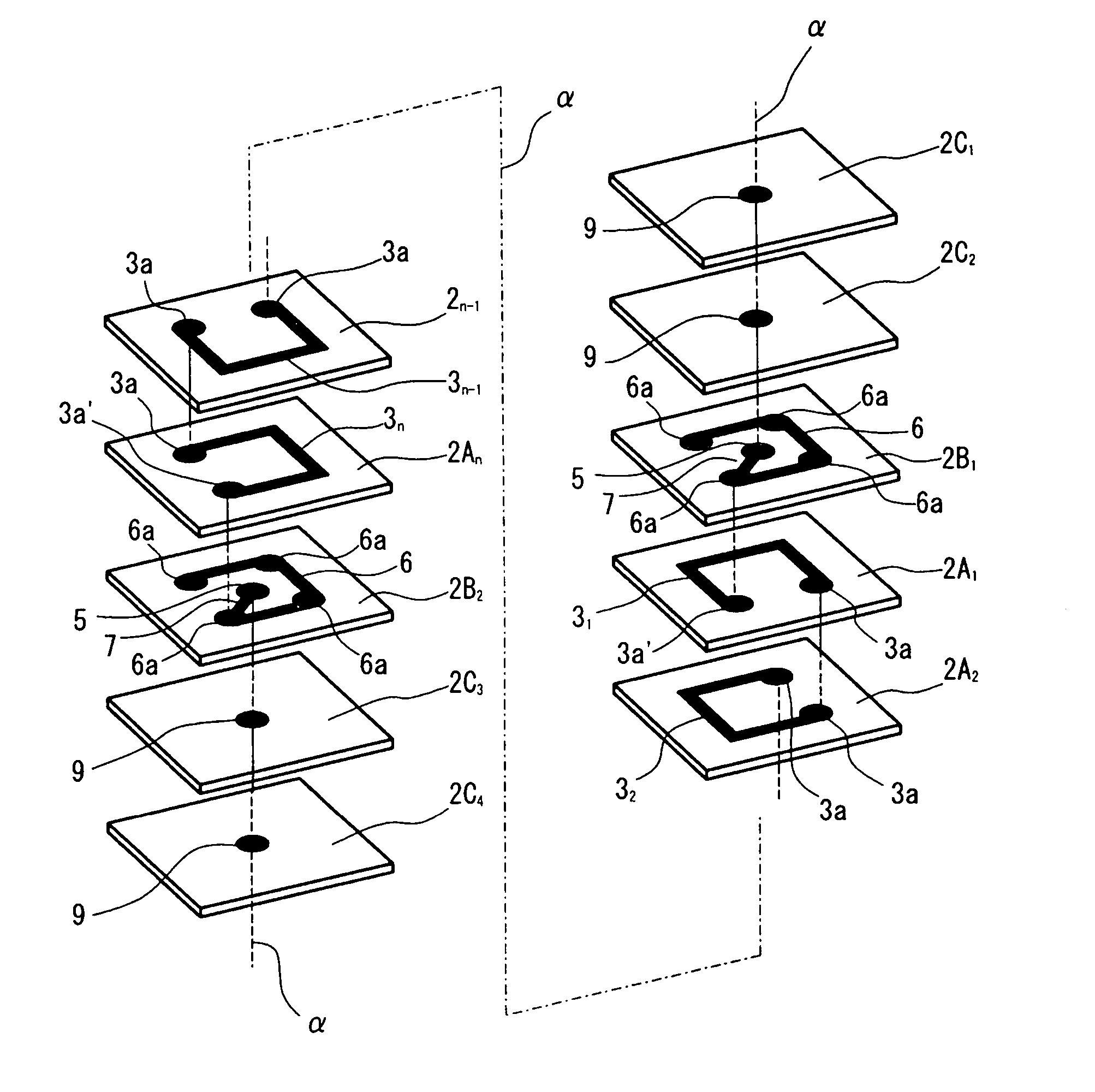
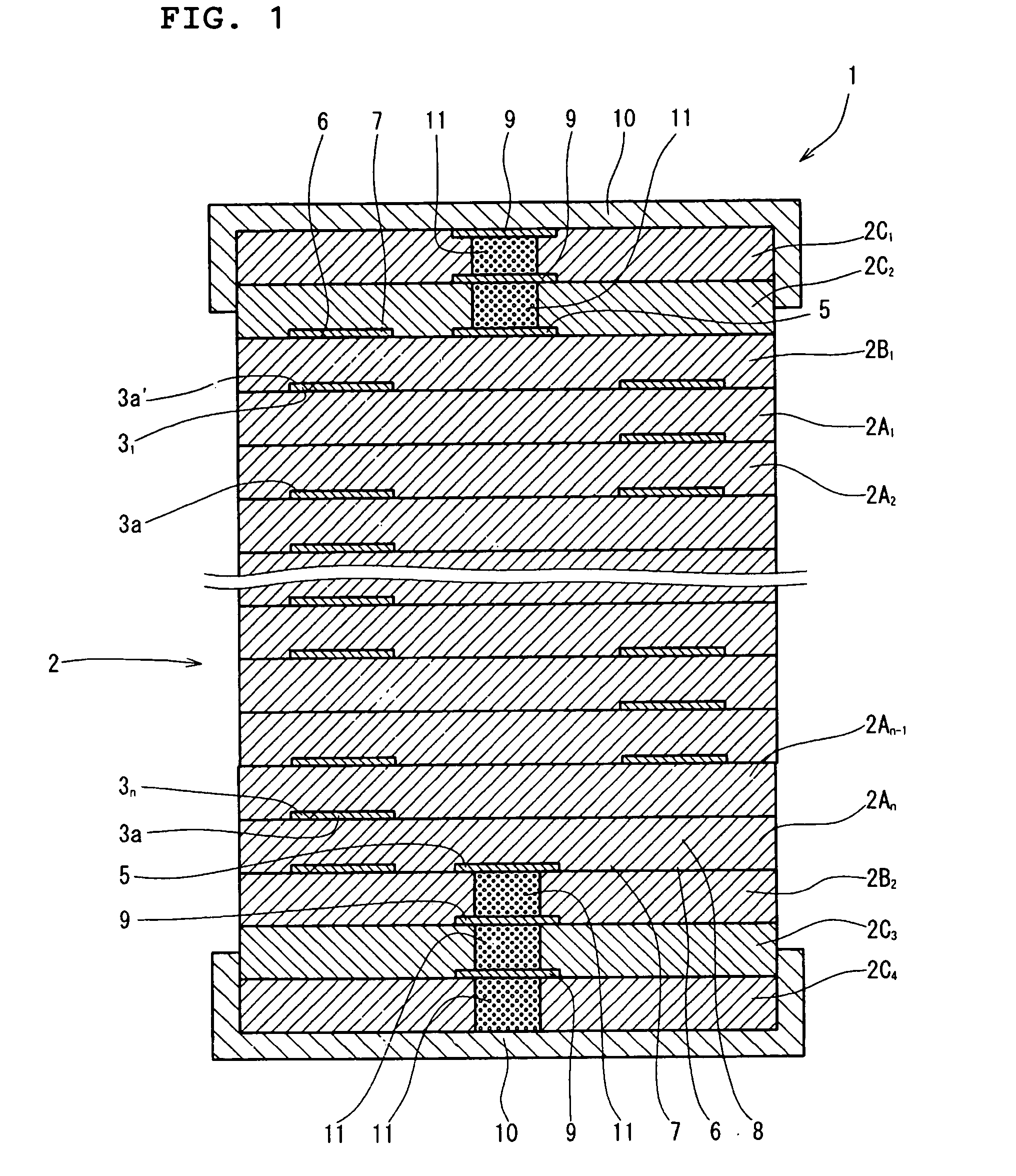
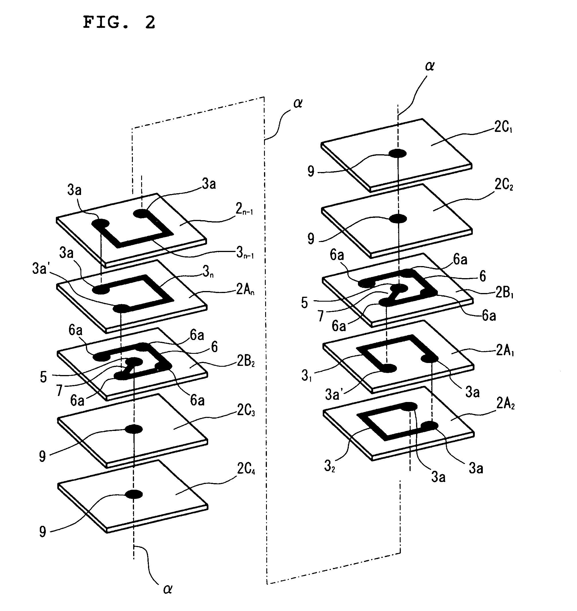
[0040] In the present preferred embodiment, the present invention relates to a multilayered chip inductor 1. FIG. 1 is a sectional view thereof. FIG. 2 is an exploded perspective view of the main portion thereof. FIG. 4 is a development view of each ceramic layer forming the multilayered chip inductor 1.

[0041] The multilayered chip inductor 1 has a plurality of first ceramic layers 2A1 to n, second ceramic layers 2B1 and 2, and coated ceramic layers 2C1 to 4 preferably having a substantially rectangular shape or a substantially square shape. The ceramic layers 2A1 to n and 2B1 and 2 and the coated ceramic layers 2C1 to 4 are laminated in sequence in an integral manner to form a arranged on one end of the laminate, and the second ceramic layer 2B2 is preferably arranged on th...


PUM

PropertyMeasurementUnit
thicknessaaaaaaaaaa
annular shapeaaaaaaaaaa
rectangular shapeaaaaaaaaaa

Abstract

A multilayered electronic component that is easy to manufacture and that has excellent electrical characteristics includes end portions of coil wiring patterns that oppose a coil connection electrode that is displaced on the surface of a second ceramic layer due to an increase or decrease in the number of first ceramic layers. A coil connection electrode has a shape in which surface portions of second ceramic layers or opposed second ceramic layers having the first ceramic layers disposed in between are connected to the end portions of the coil wiring patterns that oppose the respective coil connection electrode, which are displaced due to the increase or decrease in the number of the first ceramic layers. A connection wiring pattern has a shape in which one portion of a coil connection electrode is connected to one portion of an external extension electrode connection pattern.

Description

BACKGROUND OF THE INVENTION [0001] 1. Field of the Invention [0002] The present invention relates to a multilayered electronic component having a coil conductor formed inside a laminate. [0003] 2. Description of the Related Art [0004] An example of conventional multilayered electronic components is shown in FIGS. 13 and 14. This multilayered electronic component 100 is a chip inductor, and a coil conductor 102 is buried inside a laminate 101 having a rectangular parallelepiped shape. The coil conductor 102 includes a coil wiring pattern 104 formed on the surface of a ceramic layer 103 forming the laminate 101, and an electrical conductor (via conductor) 105 arranged on each ceramic layer 103 so as to extend therethrough in the thickness direction thereof. The coil conductor 102 functions as a coil by electrically connecting the end portions of each coil wiring pattern 104 by an electrical conductor 105. [0005] An external extension of the coil conductor 102 is formed in the followin...

Claims


Application Information

Patent Timeline
Patent Type & Authority Applications(United States)
IPC IPC(8): H01F41/04H01F17/00H01F17/03
CPCH01F17/0013H01F2017/002Y10T29/4902Y10T29/49073Y10T29/4913Y10T29/49155Y10T29/49002Y10T29/49078Y10T29/49071H01F17/03
Inventor MAEDA, TOMOYUKIMATSUSHIMA, HIDEAKI
Owner MURATA MFG CO LTD
Why Eureka
Try Eureka