Thin film magnetic head and manufacturing method thereof

a technology of thin film and magnetic head, which is applied in the construction of head windings, instruments, data recording, etc., can solve the problems of submicron process accompanied by problems, degradation of write ability, and various problems to be solved in the writing element, so as to reduce the resistance of the coil and the quantity of generated heat, the effect of increasing the sectional area and increasing the number of coil turns

Active Publication Date: 2005-06-16
HEADWAY TECH INC +1
View PDF11 Cites 17 Cited by
  • Summary
  • Abstract
  • Description
  • Claims
  • Application Information

AI Technical Summary

Benefits of technology

[0044] The second insulating film between the first coil and the second coil can be formed as a very thin Al2O3 film of about 0.1 μm in thickness by applying chemical vapor deposition (hereinafter, referred to as CVD) or the like. Therefore, it is possible to maximize the sectional area of the first and second coils between the back gap portion and the first pole portion, and consequently decrease the resistance of the coils and the quantity of generated heat as keeping the number of coil turns. This makes it possible to suppress occurrence of a thermal protrusion in a pole portion, and consequently avoid a head crash and the damage or destruction of a magnetic record on a magnetic recording medium and meet a demand for a low floating height for a high recording density.
[0045] As one of the first coil and the second coil is fitted into the space between coil turns of the other, insulated from the coil turns of the other by the second insulating film, high wiring density of coil conductors is achieved. This makes it possible to shorten the yoke length YL as keeping the same number of coil turns.

Problems solved by technology

On the other hand, the improvement in performance of a write element has various problems to be solved as described below.
However, this submicron process is accompanied by the problems as described below.
First, the narrower the structure of a pole portion is made in a track structure, the more the pole portion is liable to cause a magnetic saturation, with degradation in a write ability.
Among them, FeN, CoFeN and the like show a high saturation magnetic flux density of 2.4 T, for example, but they are difficult to form a pattern by plating, and consequently it becomes necessary to form a film of the material by sputtering and subsequently to pattern the film by ion milling.
In case of a sputtering film as thick as 0.2 μm or more, accurate control over a track width of 0.2 μm or less, however, is very difficult, concerned with a mask made of photoresist or a mask formed of a magnetic film to form an upper pole.
However, the seed film is, for example, a sputtering film of CoFe, and thus is very difficult to trimmed by ion beam.
The upper pole having such a thin film thickness causes a magnetic saturation in a write operation, with considerable degradation in an overwrite characteristic.
Thus the upper pole reduces in volume and the reduction in volume increases a risk of a magnetic saturation.
Furthermore, the pole is narrowed to have a taper angle making the width gradually smaller from the flare point toward the ABS, causing a problem that the track width varies according to individual thin film magnetic heads.
And while a narrow-track structure might be achieved by applying a semiconductor process technique on a flat pole structure to perform a submicron process on a pole portion, the surface of a flare portion expanding in width from the pole portion toward the yoke portion forms the same plane as the surfaces of the pole portion and yoke portion, causing problems that, in a write operation, the magnetic flux leaked from a side of the flare portion might erase a magnetic record on an adjacent track in a magnetic recording medium (side erase phenomenon), give a magnetic record to an adjacent track in a magnetic recording medium (side write phenomenon), or the like.
Due to these problems, it is difficult to perform an accurate track control of 0.2 μm or less, and consequently it is impossible to achieve a high surface recording density of 100 Gb / p or more.
On the other hand, in case of reducing the width of a coil without reducing the number of coil turns, the electric resistance of the coil increases, so a temperature rise due to heat generation in a write operation increases.
When a thermal protrusion occurs, the part where the thermal protrusion has occurred comes into contact with a magnetic recording medium in write and read operations, causing head crash, damage or destruction of a magnetic record on the magnetic recording medium.
If it is impossible to avoid a thermal protrusion, the floating height of a thin film magnetic head must be increased after all, which makes it impossible to meet a demand for a low floating height for a high recording density.

Method used


Image

  • Thin film magnetic head and manufacturing method thereof
  • Thin film magnetic head and manufacturing method thereof
  • Thin film magnetic head and manufacturing method thereof

Examples


embodiment 1

(1) Embodiment 1

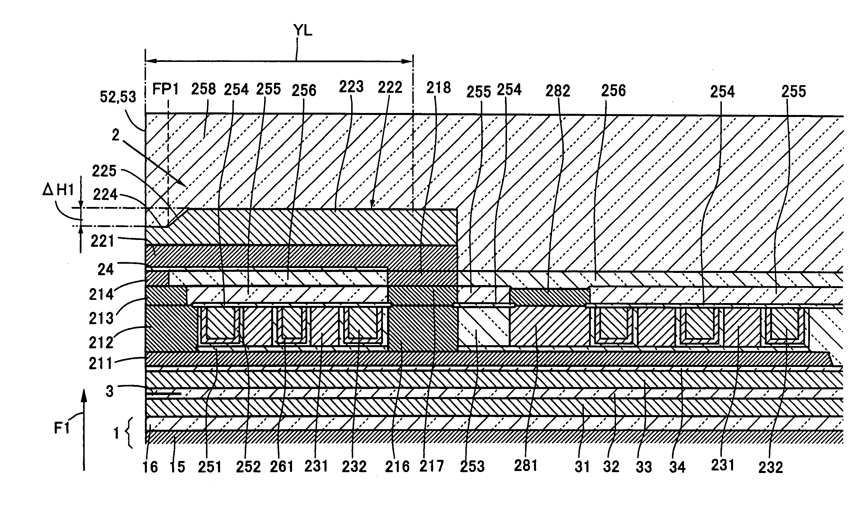
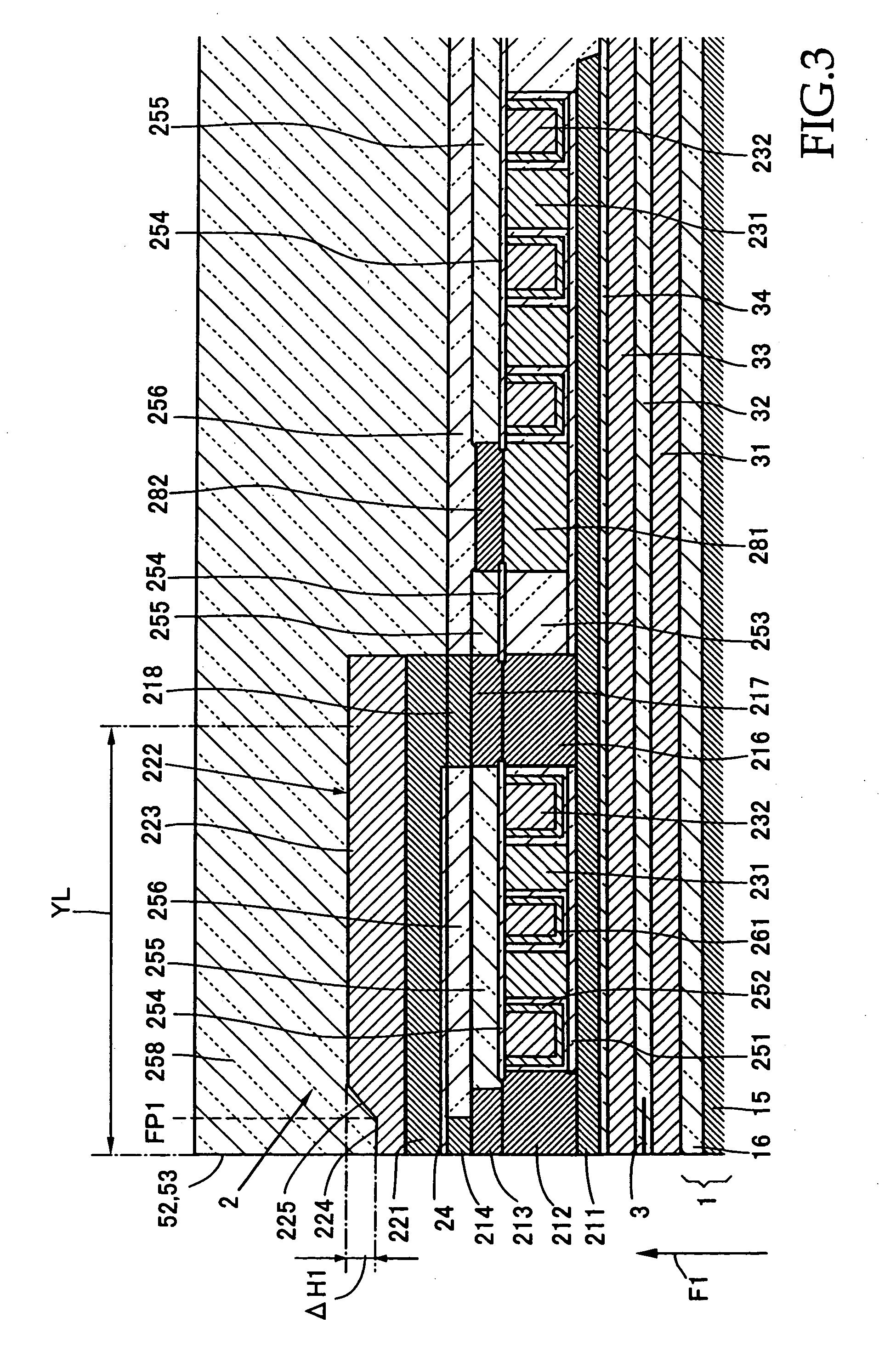
[0173] Embodiment 1 related to a manufacturing method is a process of manufacturing a thin film magnetic head of a first aspect having a first coil 231 and a second coil 232 (FIGS. 1 to 6). It is notified in advance that processes illustrated in FIGS. 11 to 44 are performed on a wafer.

[0174] First, referring to FIG. 10, on an insulating film 16 deposited on a base body 15 there are formed a first shield film 31, a read element 3, an insulating film 32, a second shield film 33, an insulating film 34 and a first magnetic film 211 by means of publicly known processes. After that, an insulating film 251 is formed on the flat surface of the first magnetic film 211, the insulating film 251 having an area slightly larger than an area necessary for forming a coil, and then a seed film 260 is formed on the surface of the insulating film 251. The seed film 260 is formed so as to cover the surface of the insulating film 251 and the surface of the first magnetic film 211. The s...

embodiment 2

(2) Embodiment 2

[0217] Embodiment 2 relates to a method for manufacturing a thin film magnetic head shown in FIGS. 7 and 8. FIGS. 47 to 65 show a process of manufacturing the same. It is notified in advance that processes illustrated in FIGS. 47 to 63 are also performed on a wafer.

(A) Process Leading to a State of FIG. 47.

[0218] Referring to FIG. 47, on an insulating film 16 deposited on a base body 15 there are formed a first shield film 31, a read element 3, an insulating film 32, a second shield film 33, an insulating film 34 and a first magnetic film 211 by means of publicly known processes.

[0219] The first magnetic film 211 can be made of a plating film of NiFe (80%:20%), NiFe (45%:55%) or CoNiFe. The first magnetic film 211 may be made of a sputtering film of FeAlN, FeN, FeCo, CoFeN, FeZrN or the like with a thickness of 0.5 to 0.6 μm.

[0220] After that, an insulating film 251 is formed, for example, 0.2 μm thick on the flat surface of the first magnetic film 211, the insu...

embodiment 3

(3) Embodiment 3

[0250] Embodiment 3 is a process of manufacturing a thin film magnetic head shown in FIG. 9, and is illustrated in FIGS. 66 to 71. Processes, which have been illustrated and described in embodiment 1 or 2 and are also applied to embodiment 3, are referred to the description of embodiment 1 or 2 and the illustrations of the processes may be omitted.

(A) Process Leading to a State of FIG. 66

[0251] On an insulating film 16 deposited on a base body 15 there are formed a first shield film 31, a read element 3, an insulating film 32, a second shield film 33, an insulating film 34 and a first magnetic film 211 by means of publicly known processes. After that, an insulating film 251 is formed on the flat surface of the first magnetic film 211, the insulating film 251 having an area slightly larger than an area necessary for forming a coil. The insulating film 251 is formed so as to have openings in parts where a back gap portion and a pole portion are to be formed. After th...


PUM

PropertyMeasurementUnit
saturation magnetic flux densityaaaaaaaaaa
widthaaaaaaaaaa
saturation magnetic flux densityaaaaaaaaaa

Abstract

The invention is directed to improvement of a write element of a thin film magnetic head. In said write element, a first coil and a second coil are provided on a first insulating film formed on one surface of a first magnetic film and surround in a spiral form a back gap portion. A second yoke portion in the upper position comprises a wide portion, a narrow portion and a sloping flare portion. The wide portion has a flat surface and is connected to the first magnetic film by a back gap portion at the rear of the medium-facing surface. The narrow portion forms the second pole portion and the surface of the narrow portion being at a lower position than the surface of the wide portion. The sloping flare portion extends from the narrow portion to the wide portion, gradually increasing in width and its surface sloping upward away from the surface of the narrow portion to the surface of the wide portion.

Description

BACKGROUND OF THE INVENTION [0001] 1. Field of the Invention [0002] The present invention relates to a thin film magnetic head, a magnetic recording device using the same and a method for manufacturing the same, and particularly to improvement of a write element provided in a thin film magnetic head. [0003] 2. Discussion of Background [0004] In recent years, the improvement in performance of a thin film magnetic head is demanded with the improvement in surface recording density of a hard disk device. The improvement in performance of a thin film magnetic head must be achieved in two aspects. One aspect is the improvement in performance of a read element, and the other is the improvement in performance of a write element. [0005] The performance of a read element has been remarkably improved by development and practical use of a GMR (giant magnetoresistive) head provided with a spin valve film (SV film) or a ferromagnetic tunnel junction. Recently, this trend is so vigorous as to exce...

Claims


Application Information

Patent Timeline
Patent Type & Authority Applications(United States)
IPC IPC(8): G11B5/147G11B5/39
CPCG11B5/3903
Inventor SASAKI, YOSHITAKAKAMIGAWA, TAKEHIROITOH, HIROYUKIISHIZAKI, KAZUOTANEMURA, SHIGEKIARAKI, HIRONORI
Owner HEADWAY TECH INC
Why Eureka
Try Eureka