

Method of forming a memory device having a storage transistor
a memory device and storage transistor technology, applied in semiconductor devices, digital storage, instruments, etc., can solve the problems of difficult to provide access transistors with good off-state leakage characteristics, difficult to provide capacitors in a small area with sufficient capacitance, and capacitor-less cells can suffer from poor performance characteristics of retention time, access time, distribution characteristics, reliability,
- Summary
- Abstract
- Description
- Claims
- Application Information
AI Technical Summary
Benefits of technology
Problems solved by technology
Method used
Image

Examples
Embodiment Construction
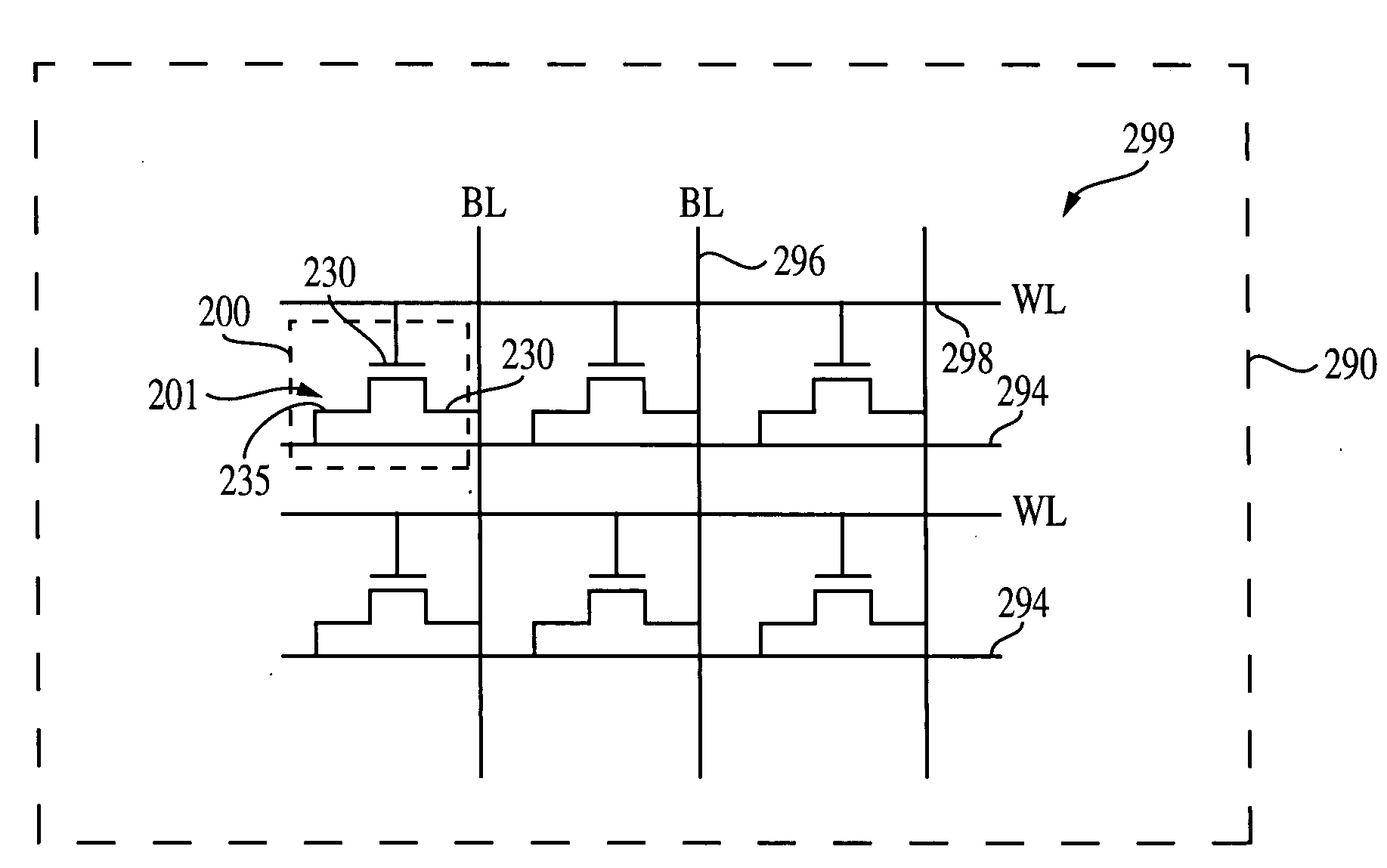
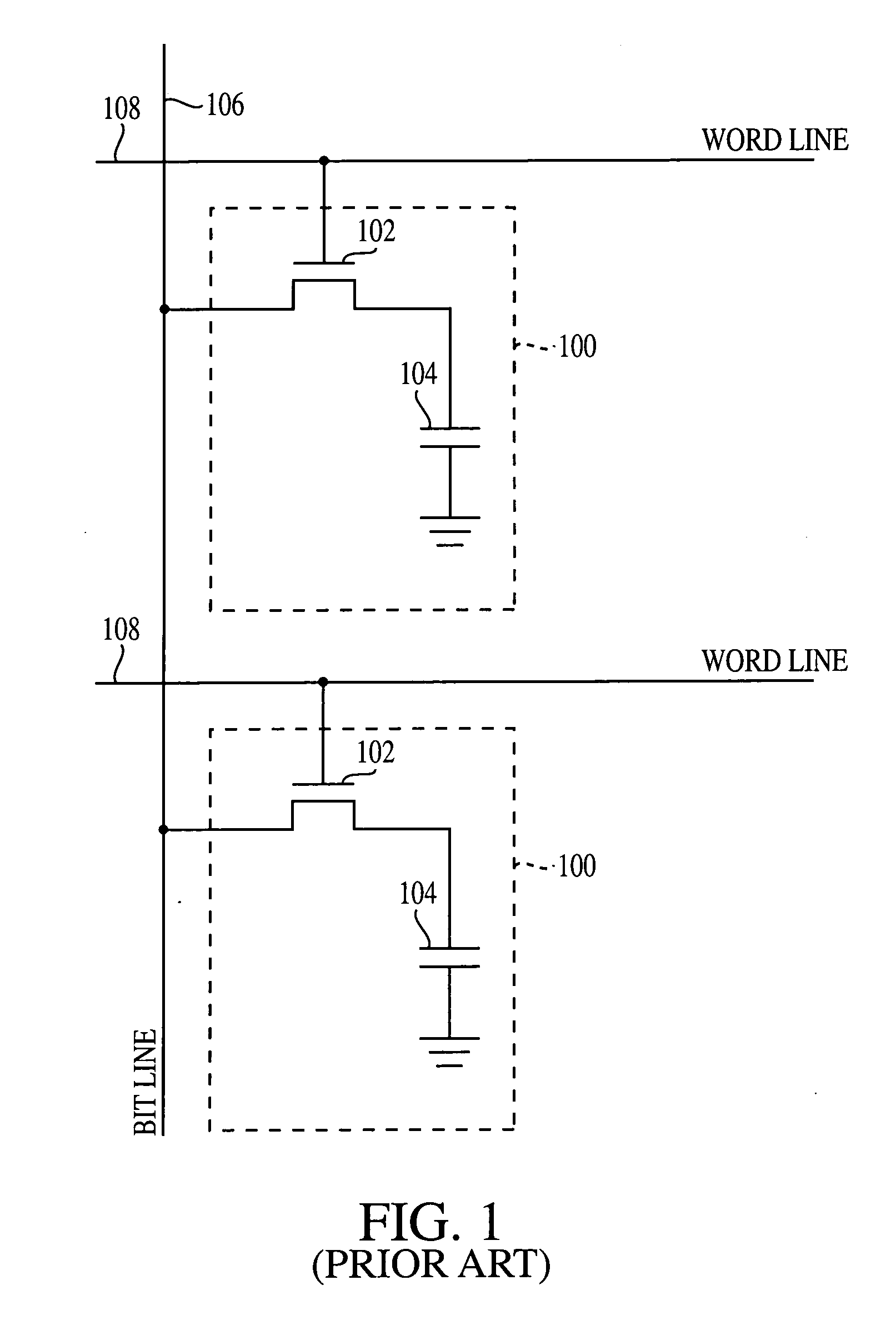
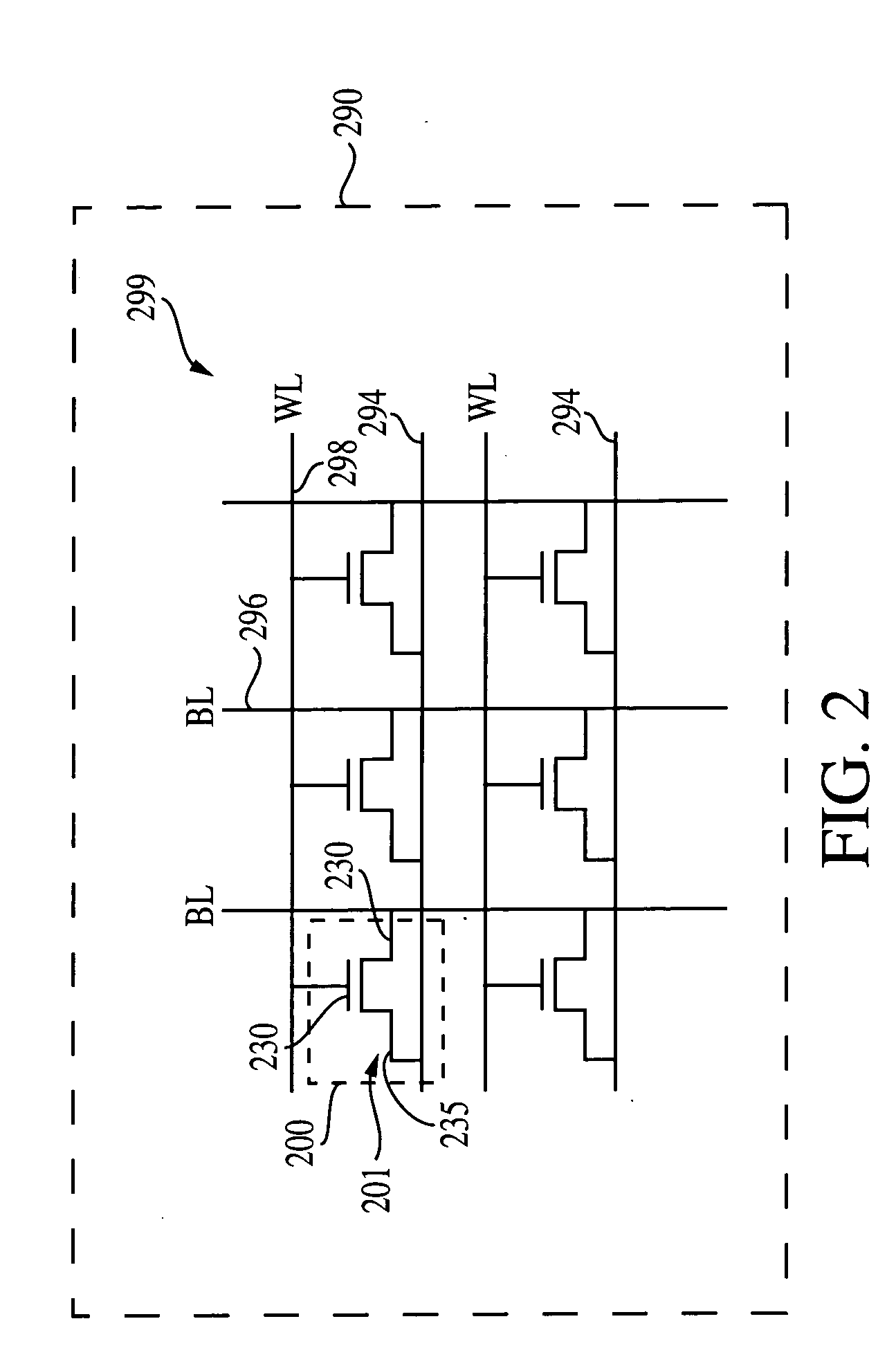
[0030] In the following detailed description, reference is made to the accompanying drawings, which form a part hereof and illustrate specific embodiments in which the invention may be practiced. In the drawings, like reference numerals describe substantially similar components throughout the several views. It is noted that the drawings of the invention are not to scale. The drawings are intended to depict only exemplary embodiments of the invention and, therefore, should not be considered as limiting the scope of the invention. These embodiments are described in sufficient detail to enable those skilled in the art to practice the invention, and it is to be understood that other embodiments may be utilized, and that structural, logical, and electrical changes may be made without departing from the spirit and scope of the present invention.
[0031] The terms “wafer” and “substrate” are to be understood as including silicon, silicon-on-insulator (SOI), silicon-on-sapphire (SOS), and si...
PUM
 Abstract
Description
Claims
Application Information