Method of manufacturing plasma display panel and method of manufacturing plasma display apparatus

Inactive Publication Date: 2005-06-16
PANASONIC CORP
View PDF4 Cites 24 Cited by
  • Summary
  • Abstract
  • Description
  • Claims
  • Application Information

AI Technical Summary

Benefits of technology

[0073] By forming the plasma display apparatus in a modular fashion, it is possible to carry out repairs simply and rapidly by replacing individual modules, if the need to replace a component arises.
[0074] The first object is achieved because it is possible to reduce the time required for baking processes by means of simultaneous baking, and hence manufacturing costs can be reduced. Also, since the glass frit in the metal paste has a softening point equal to or lower than that of the glass frit in the glass paste, and the content ratio of the glass frit in the metal paste is set to a suitable value, it is possible to prevent the metal from dispersing into the dielectric layer during baking, and hence discoloration of the dielectric layer is avoided and good display quality can be maintained.
[0075] The second object is achieved because it is possible to reduce the time required for baking processes by means of simultaneous baking, and hence manufacturing costs can be reduced. Also, since the content ratio of the glass frit in the metal paste is set to a suitable value, the metal paste layer becomes conductive upon drying and therefore electrical inspection of the electrode layer, for example, can be performed before forming the glass paste layer. If any faults, such as disconnections, or the l

Problems solved by technology

Normally, if a glass sheet is cooled rapidly, deformation or distortion will be left in the glass sheet due to uneven cooling, and hence the glass may fracture or suffer from uneven shrinkage upon baking.
Considering that the cells emitting red, green and blue light in a 42-inch VGA class display apparatus are approximately 350 μm in size, this extent of deformation of the glass substrate caused by sudden cooling is a critical problem in plasma display apparatus.
If a baking oven of this kind is required for each of the baking processes illustrated in FIG. 17, then the installation surface area and power consumption required for the baking oven will be huge, the building accommodating the plasma display apparatus mass-production plant will inevitably be very large, energy consumption will be huge

Method used


Image

  • Method of manufacturing plasma display panel and method of manufacturing plasma display apparatus
  • Method of manufacturing plasma display panel and method of manufacturing plasma display apparatus
  • Method of manufacturing plasma display panel and method of manufacturing plasma display apparatus

Examples


first embodiment

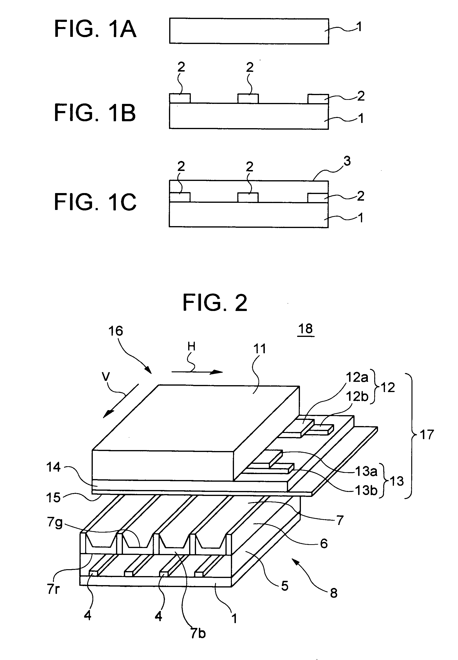
[0097] A first embodiment is described with reference to FIG. 1A to FIG. 5. FIG. 1A to FIG. 1C are a series of process diagrams for describing a method of manufacturing a plasma display panel 18 according to a first embodiment of the present invention. FIG. 2 is a perspective view, schematically showing the inner structure of the plasma display panel 18.

[0098] In the method of manufacturing the plasma display panel 18 according to this embodiment, suitable values are set for the manufacturing conditions, such as the content ratio of the glass frit in the silver paste, the relationship between the softening points of the glass frits in the silver paste and the glass paste, and the average particle size of the silver powder. Then, an address electrode pattern and a dielectric layer pattern are formed and both patterns are baked (calcined) simultaneously, thereby forming a rear surface substrate. A front surface substrate is manufactured by means of a conventional method that does not...

second embodiment

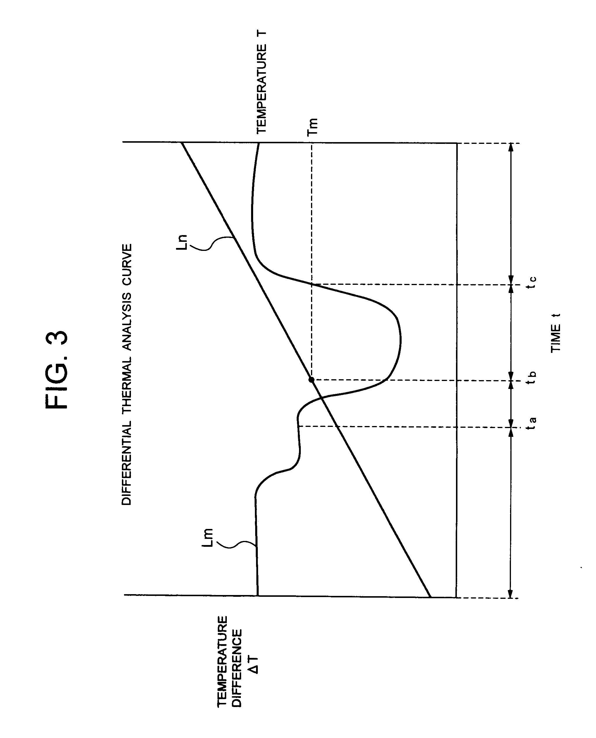
[0144]FIG. 6A to FIG. 6D are a series of process diagrams for describing a method of manufacturing a plasma display panel according to a second embodiment of the present invention. FIG. 7 to FIG. 10 show the relationship between the baking conditions and transmissivity of the front surface substrate, respectively. FIG. 11 illustrates the characteristics of colored light from a plasma display apparatus using the plasma display panel. FIG. 12 shows the relationship between the baking temperature and the b* value of the front surface substrate.

[0145] The main point of difference of this embodiment with respect to the first embodiment lies in the fact that in the manufacture of the front surface substrate, appropriate manufacturing conditions are established with regard, for instance, to the content of glass frit in the silver paste, the relationship between the softening points of the glass frit in the silver paste and the glass paste, the average particle size of the silver powder, a...

third embodiment

[0217]FIG. 13A to FIG. 13E are a series of process diagrams showing a method of manufacturing a plasma display panel according to a third embodiment of the invention, and FIG. 14 is a plan diagram schematically depicting the composition of the rear surface substrate of this plasma display panel.

[0218] The major difference between this embodiment and the first embodiment lies in the fact that the partitions are also formed simultaneously by baking.

[0219] With this exception, the third embodiment is substantially the same as the first embodiment, and hence only a brief description is given to common parts.

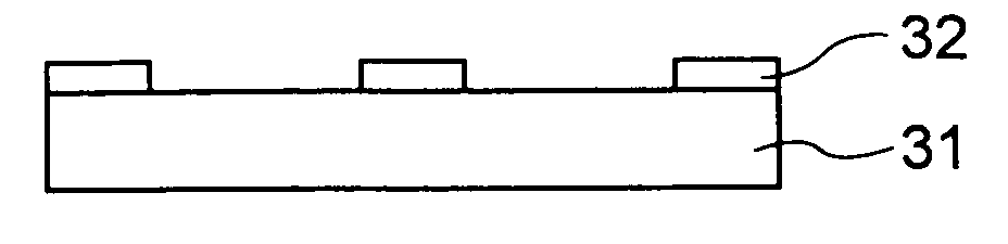
[0220] In the method of manufacturing the plasma display panel according to this embodiment, firstly, a rear surface glass substrate 31 is prepared as illustrated in FIG. 13A. Similar to the first embodiment, glass having a high strain point, for example, may be used for the rear surface glass substrate 31, but the type of glass used is not limited in particular.

[0221] Next, as s...


PUM

PropertyMeasurementUnit
Temperatureaaaaaaaaaa

Abstract

Address electrode patterns are formed on a rear surface glass substrate using a silver paste for forming address electrodes, and these patterns are dried. The average particle size of the silver powder in the silver paste is approximately 10 nm, and the softening point of the glass frit is approximately 420° C. The content ratio of the glass frit in the silver paste is set to 5 wt %. Then, a dielectric layer pattern is formed by using glass paste for forming a white dielectric layer so as to cover the address electrode patterns, and this dielectric layer pattern is dried. The glass frit in the glass paste has a softening point of approximately 540° C. Then, the address electrode patterns and the dielectric layer patterns are baked at a temperature of 540° C. Thus, the resin components in the address electrode patterns and the dielectric layer pattern are burnt away, and the glass frit components are softened so as to be fixed onto the rear surface glass substrate.

Description

BACKGROUND OF THE INVENTION [0001] 1. Field of the Invention [0002] The present invention relates to a method of manufacturing a plasma display panel and to a plasma display apparatus, and more particularly to, for example, a method of manufacturing a plasma display panel and a method of manufacturing a plasma display apparatus wherein electrodes and a dielectric layer are formed in the same baking (calcining) step. [0003] 2. Description of the Related Art [0004] In general, a plasma display apparatus having a plasma display panel as a main component (hereinafter, also referred to as “PDP”) has various advantages compared with a CRT (Cathode Ray Tube) display or liquid crystal display apparatus, or the like, in that it produces no flicker, has a larger display contrast ratio, greater capacity for providing a large screen in a thin unit, faster response, and the like. Therefore, in recent years, plasma display apparatus are used as large-size flat-screen television receivers, display...

Claims


Application Information

Patent Timeline
IPC IPC(8): H01J9/02H01J9/24H01J9/26H01J17/49
CPCH01J9/02H01J2211/225H01J11/38H01J11/22C03C8/02H01J9/242H01J11/12H01J11/40
Inventor OIDA, OSAMUSHINOHARA, TAKUO
Owner PANASONIC CORP
Why Eureka
Try Eureka