Nitride semiconductor light emitting device

Inactive Publication Date: 2005-06-23
SAMSUNG ELECTRONICS CO LTD
View PDF1 Cites 64 Cited by
  • Summary
  • Abstract
  • Description
  • Claims
  • Application Information

AI Technical Summary

Benefits of technology

[0023] The nitride semiconductor LED may further comprise a transparent electrode layer for redu

Problems solved by technology

A planar LED has drawbacks that an effective light emitting area is not sufficient and luminous efficiency per light emitting area is low because the flow of electric current is not uniformly distributed across the light emitting area unlike a vertical LED in which both electrodes are arranged on the top and the bottom of its light emitting structure.
Also, the current flow is directed laterally to increase drive voltage owing to large series resistance, resultantly reducing actual light emitting area.
That is, the nitride semiconductor LED has drawbacks of low current density per unit area originated from limitations of the planar structure as well as low area efficiency owing to small light emitting area.
As a result, it has been regarded very difficult

Method used


Image

  • Nitride semiconductor light emitting device
  • Nitride semiconductor light emitting device
  • Nitride semiconductor light emitting device

Examples


example

[0073] In order to examine those improved characteristics of the nitride semiconductor LED of the invention, three nitride semiconductor LED structures were fabricated with same component and thickness on rectangular sapphire substrates of approximately 1000×1000 μm size.

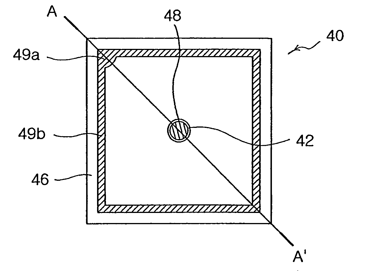
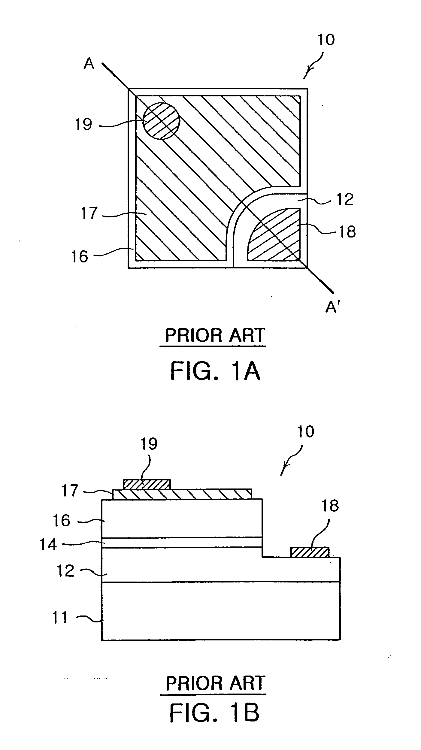
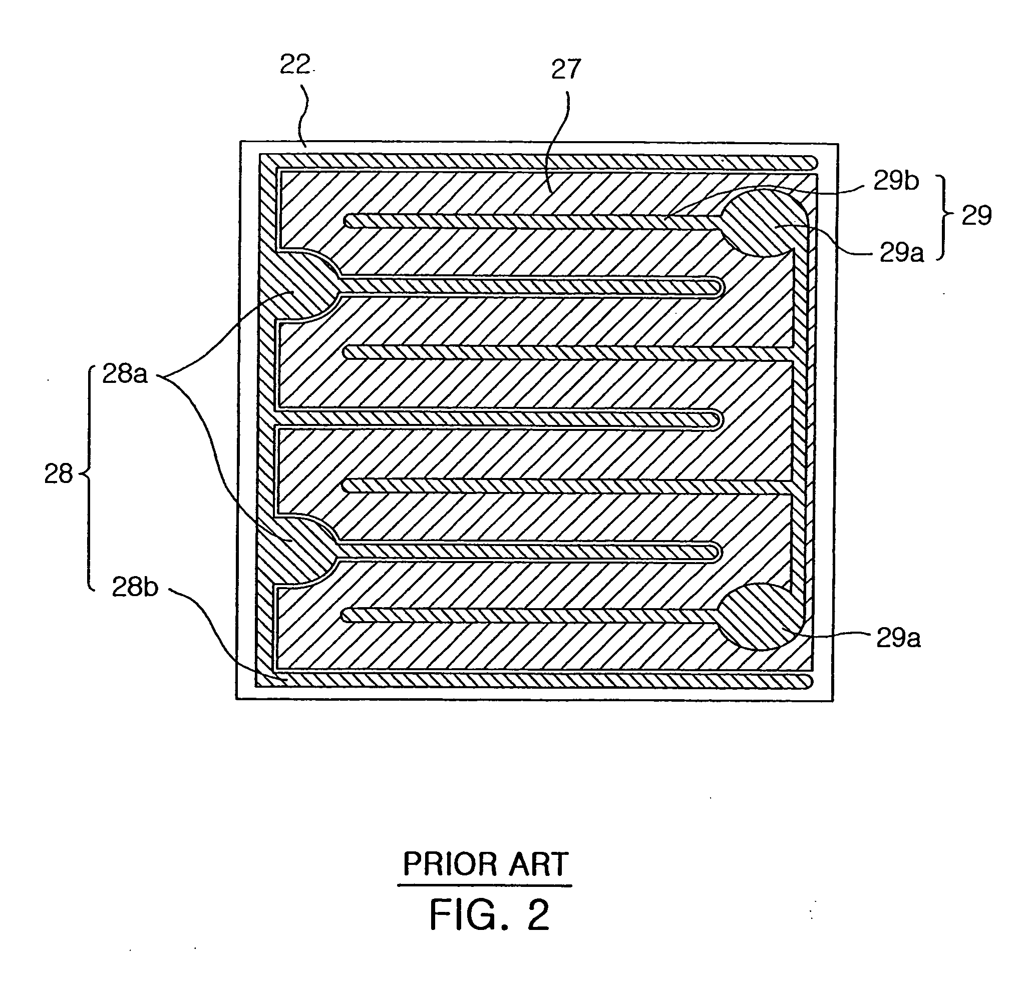
[0074] First two of the LED structures were fabricated into the nitride semiconductor LEDs of the electrode structures illustrated in FIGS. 2 and 3a, respectively. The conventional nitride semiconductor LEDs fabricated like this are illustrated in FIGS. 9a and 9b, respectively. The rest of the LED structures was fabricated to have the same electrode structure as in FIG. 8a. The nitride semiconductor LED of the invention fabricated like this is illustrated in FIG. 9c.

[0075] Although the LED of the invention shown in FIG. 9c has electrode patterns similar to those of the conventional LED shown in FIG. 9b, it has an n-electrode formed on a central area and a p-electrode formed on the upper outer periphery to surround...


PUM


Abstract

Disclosed is a nitride semiconductor LED having a light emitting structure. In the light emitting structure, an n-doped semiconductor layer has a first region and a second region surrounding the first region on a top thereof, an active layer is formed on the second region of the n-doped semiconductor layer, and a p-doped nitride semiconductor layer is formed on the active layer. A p-electrode is formed on the p-doped semiconductor layer. An n-electrode is formed on the first region of the n-doped nitride semiconductor layer.

Description

BACKGROUND OF THE INVENTION [0001] 1. Field of the Invention [0002] The present invention relates to a nitride semiconductor light emitting diode, and more particularly, a large-sized high efficiency nitride semiconductor light emitting diode which can be used suitably in a high power lighting system. [0003] 2. Description of the Related Art [0004] As well known in the art, nitride semiconductors in the form of III-V group semiconductor crystals such as GaN, InN and AlN are widely used in Light Emitting Diodes (LEDs) for emitting single wavelength light (e.g., ultraviolet ray and green light), in particular, blue light. Because a nitride semiconductor LED is fabricated on an insulation substrate such as a sapphire substrate and a SiC substrate satisfying lattice matching conditions for crystal growth, it necessarily has a planar structure in which two electrodes connected to p- and n-doped nitride semiconductor layers are arranged substantially horizontally on the top of a light emi...

Claims


Application Information

Patent Timeline
IPC IPC(8): H01L29/06H01L33/32H01L33/38H01L33/42H01L33/62
CPCH01L33/382H01L24/45H01L2224/45H01L2924/01015H01L2924/00014H01L2924/01006H01L2924/00H01L2224/48H01L2924/00011H01L2924/12041H01L24/48H01L24/16H01L24/05H01L24/06H01L2224/45099H01L2224/43H01L2224/13099H01L2924/00012
Inventor PARK, YOUNG HOCHO, HYO KYOUNGYOO, SEUNG JINKO, KUN YOO
Owner SAMSUNG ELECTRONICS CO LTD
Why Eureka
Try Eureka