Plasma display panel

Inactive Publication Date: 2005-06-23
SAMSUNG SDI CO LTD
View PDF52 Cites 22 Cited by
  • Summary
  • Abstract
  • Description
  • Claims
  • Application Information

AI Technical Summary

Benefits of technology

[0024] The extension electrodes of a pair of display electrodes corresponding to each of the discharge cells form different gaps G1 and G2 from each

Problems solved by technology

If total or partial pressure is increased to improve the efficiency, the breakdown voltage necessarily increases and the discharge instability increases.
Sometimes the discharge itself does not take place, and the use of high pressure resistant devices causes an increase in the unit cost of a circuit.
However, simply decreasing the gap between discharge electrodes may cause several problems.
One problem arising when this gap is decreased is that the discharge path is decreased, thereby deteriorating the emission efficiency of panel.
Another problem which can occur when the gap between the discharge elec

Method used


Image

  • Plasma display panel
  • Plasma display panel
  • Plasma display panel

Examples


Embodiment Construction

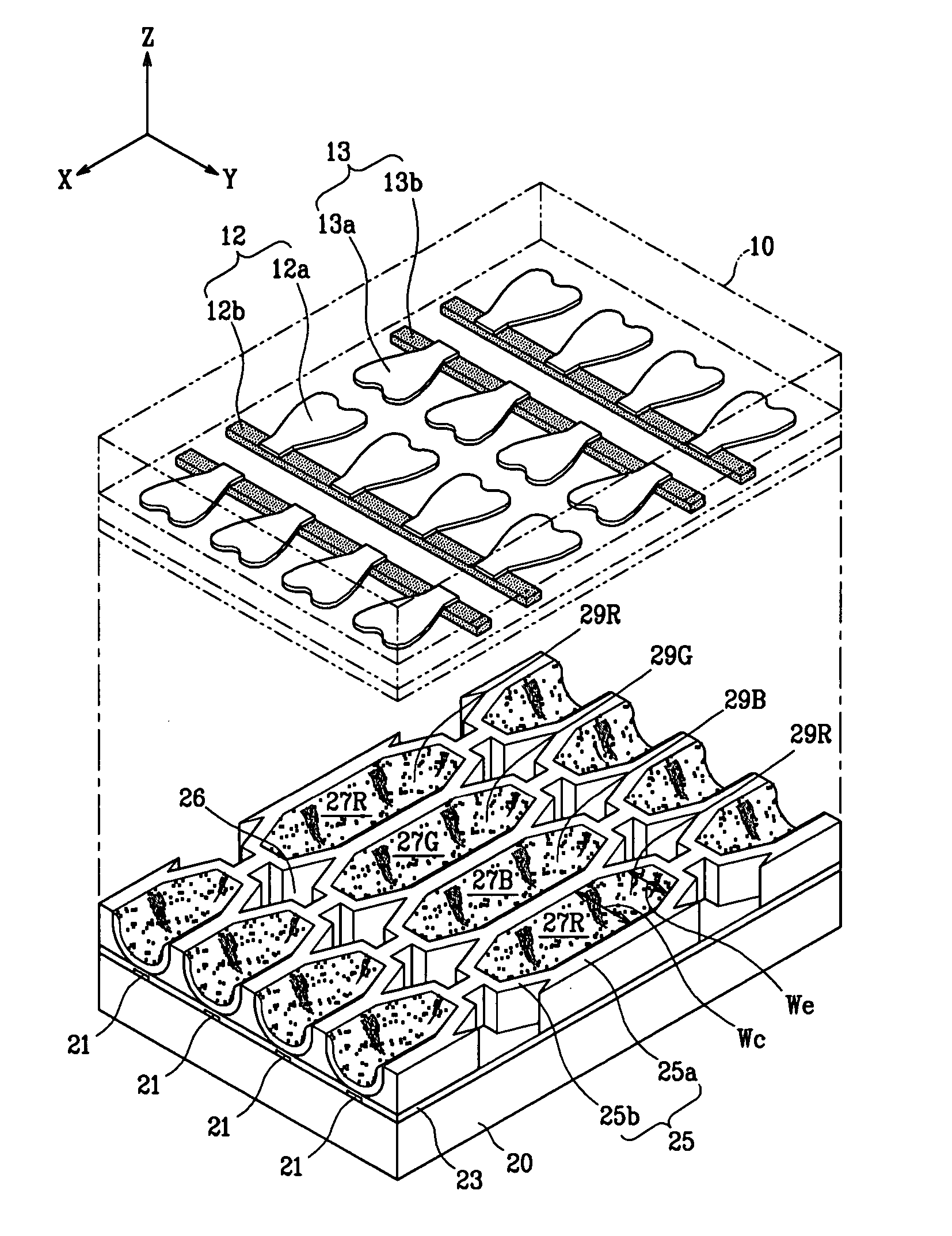
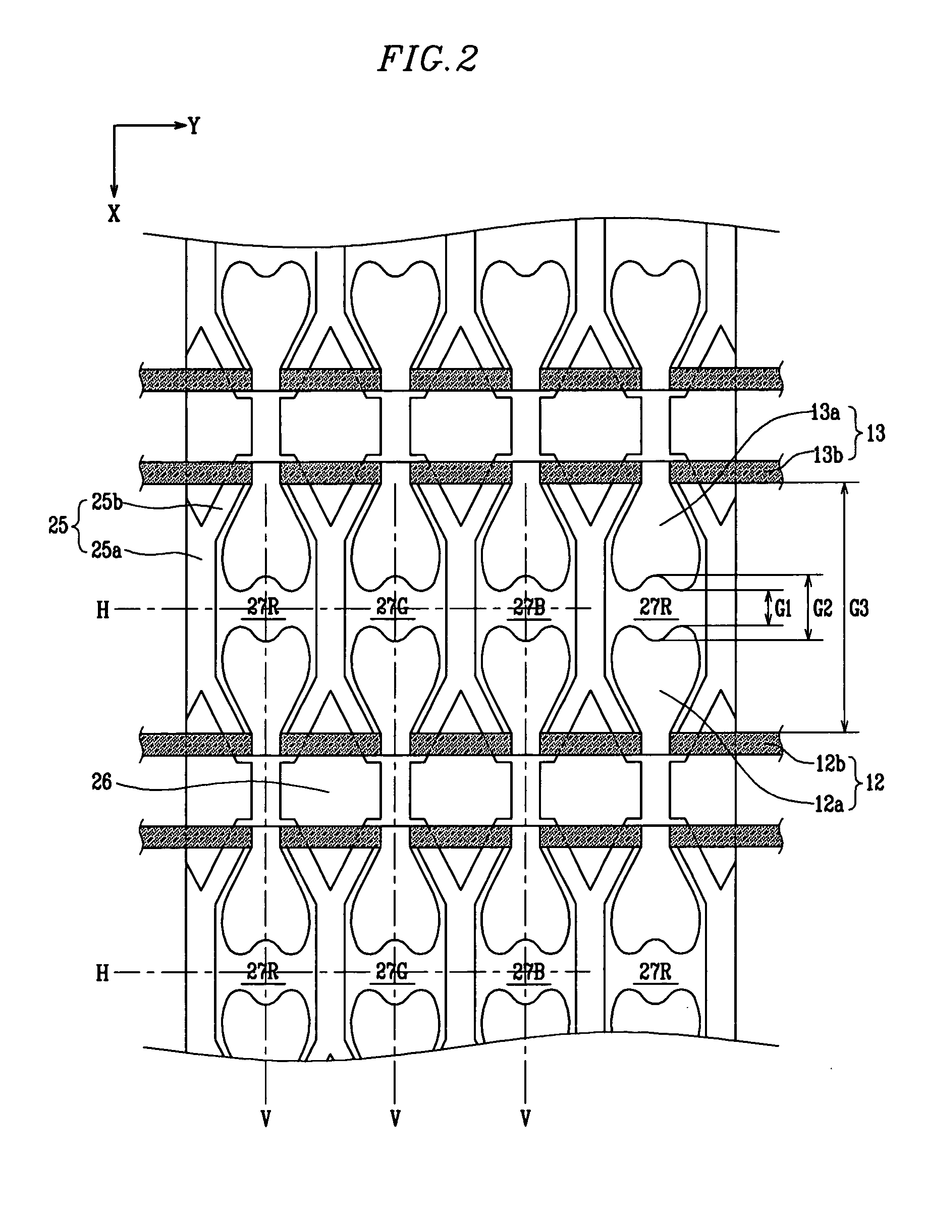
[0038] As shown in FIGS. 1-2, the plasma display panel according to one embodiment of the present invention is generally formed with a first substrate 10 and a second substrate 20 which are spaced at a predetermined distance while facing each other. In the space between both of the substrates 10, 20, a plurality of discharge cells 27R, 27G, 27B are defined by barrier ribs to cause a plasma discharge. Display electrodes 12, 13 and address electrodes 21 are formed on the first substrate 10 and the second substrate 20, respectively.

[0039] A plurality of the address electrodes 21 are formed along one direction (the X-axis direction, as shown) of the second substrate 20 on a surface of the second substrate 20 opposing the first substrate 10. The address electrodes 21 are formed in a stripe pattern and spaced apart from the adjacent address electrodes 21 at a predetermined distance and parallel to one another. A dielectric layer 23 is also formed on the second substrate 20 where the addr...


PUM


Abstract

A plasma display panel includes a first substrate, on which discharge sustain electrodes are formed, and an opposing second substrate, on which address electrodes are aligned in a first direction. Barrier ribs between the substrates define a plurality of discharge cells within which phosphor layers are formed. The display electrodes have bus electrodes, forming a corresponding pair within each of the discharge cells, and extension electrodes, extending from the bus electrodes into each of the discharge cells to form an opposing pair. A pair of the display electrodes corresponding to each of the discharge cells forms a first gap and a second gap having different distances from each other between the opposing extension electrodes, and forms a third gap between the bus electrodes. The second gap is longer than the first gap, and the third gap is longer than the second gap.

Description

CROSS REFERENCE TO RELATED APPLICATION [0001] This application claims priority to and the benefit of Korean Patent Application number 10-2003-0086144, filed Nov. 29, 2003, the entire disclosure of which is incorporated herein by reference. BACKGROUND OF THE INVENTION [0002] (a) Field of the Invention [0003] The present invention relates to a plasma display panel (hereinafter, PDP), and more particularly, to a surface discharge type PDP with an electrode structure in which a pair of display electrodes are formed on one substrate and have a corresponding pair of bus electrodes within each discharge cell between two substrates to cause a display discharge. [0004] (b) Description of the Related Art [0005] Generally, a plasma display panel is a display device in which ultraviolet rays generated by gas discharge excite phosphors to realize predetermined images. Such a plasma display panel is popular for wide screen display devices since it enables the manufacture of large screen sizes wit...

Claims


Application Information

Patent Timeline
IPC IPC(8): H01J17/04H01J17/49
CPCH01J11/12H01J11/24H01J2211/323H01J2211/245H01J11/32
Inventor KWON, JAE-IKKWON, HYE-KYONGKANG, TAE-KYOUNGHEO, EUN-GI
Owner SAMSUNG SDI CO LTD
Why Eureka
Try Eureka