Memory access circuit for adjusting delay of internal clock signal used for memory control

Inactive Publication Date: 2005-06-23
PIONEER CORP
View PDF4 Cites 45 Cited by
  • Summary
  • Abstract
  • Description
  • Claims
  • Application Information

AI Technical Summary

Benefits of technology

[0040] According to the invention, the memory access circuit adjusts the memory access timing by using the synchronizing signal having the blanking periods in its front and rear portions, thereby advantageously adjusting the memory access timing without restricting the actual data processing.
[0041] Further, according to the invention, it is effective in performing a me

Problems solved by technology

There occurs a time deviation in signals transmitting between the both owing to a wiring delay therebetween.
Since a change in delay occurs because of these factors, it is difficult to estimate the details of a delay time taken to read out data from an external memory at a time of designing a memory access circuit.
When a reading delay from a memory and a wiring delay change from the values at a time of desig

Method used


Image

  • Memory access circuit for adjusting delay of internal clock signal used for memory control
  • Memory access circuit for adjusting delay of internal clock signal used for memory control
  • Memory access circuit for adjusting delay of internal clock signal used for memory control

Examples


first embodiment

[0057] Hereinafter, best modes for carrying out the invention will be described with reference to the drawings.

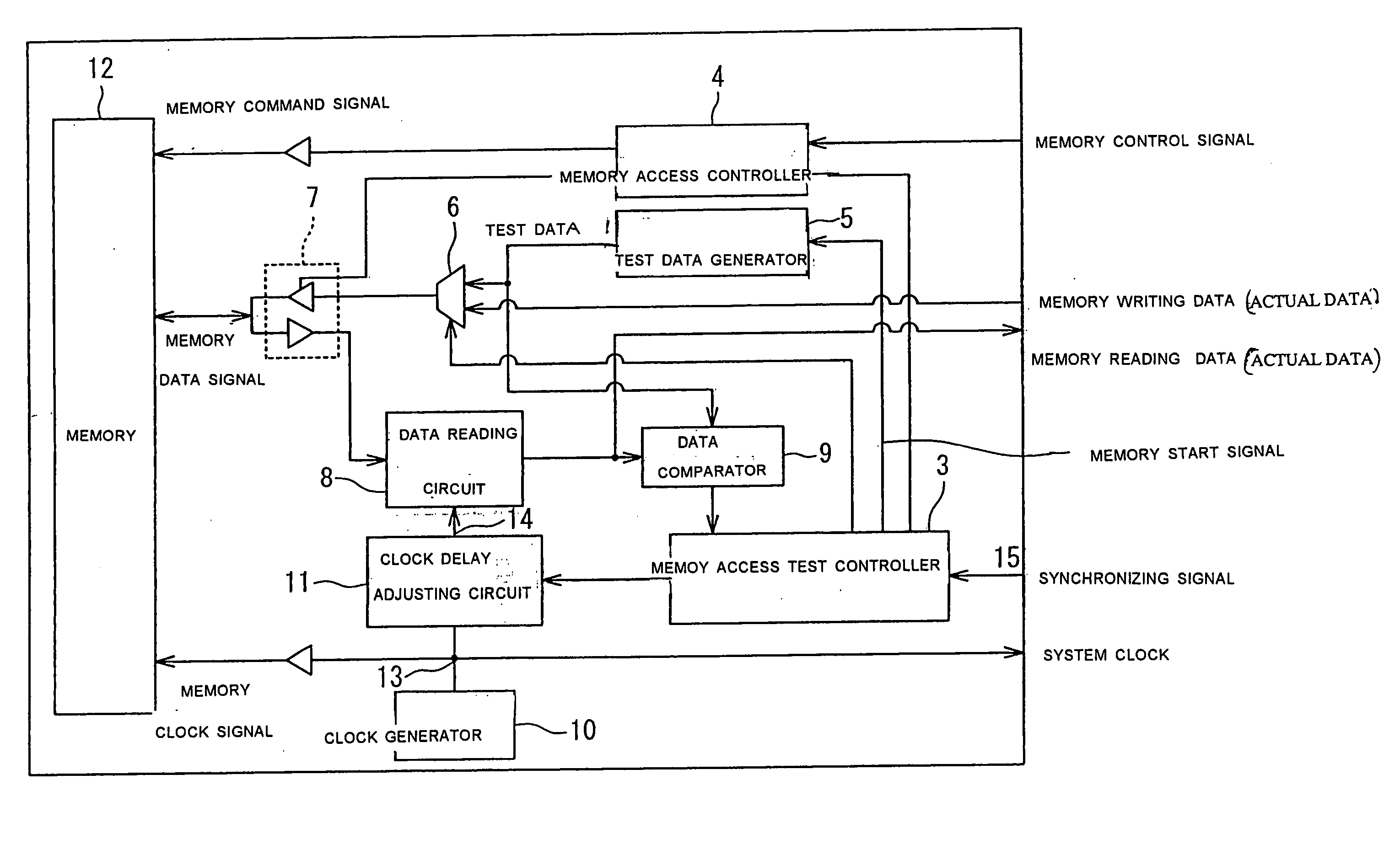
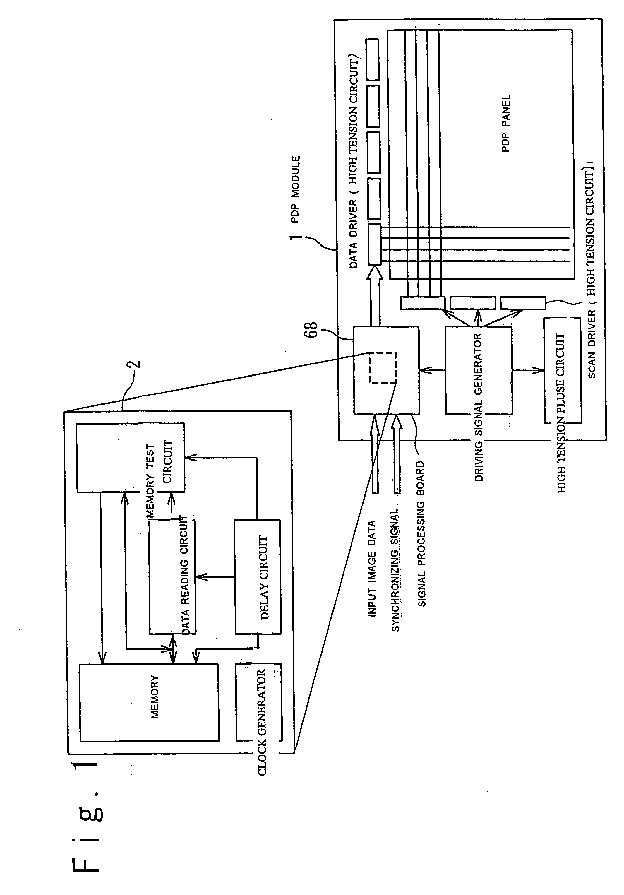
[0058]FIG. 1 is a view showing an example of a system on which a memory access circuit described in this embodiment is mounted. The device described in this embodiment works effectively on such a system that needs a frame memory of large capacity with a temperature change in its operating environment within the range of −10° C. to +80° C. and with various initial setting for power voltage in LSI. When the memory access circuit of this embodiment is mounted on, in particular, such a large-sized display system as being represented by a plasma display, it is effective in operating the system stably. In the following form of the embodiment, a description will be made in the case where the memory access circuit of the invention is mounted on a plasma display. This does not intend to restrict the system on which the memory access circuit 2 of the invention is mounted. With refer...

second embodiment

[0088] Hereinafter, a second embodiment of the invention will be described with reference to the drawings. FIG. 8 is a block diagram showing a structure of the second embodiment. A memory access circuit in the second embodiment is provided with a data delay circuit 18 in addition to the memory access circuit shown in the first embodiment. As illustrated in FIG. 8, the data delay circuit 18 is connected between the data selector 6 and the I / O buffer 7. Memory writing data is supplied to the data delay circuit 18 from the data selector 6 and writing test data is supplied there from the test data generator 5. In reply to a writing test start signal supplied from the memory access test controller 3, the data delay circuit 18 performs a data writing test. Based on the result of the writing test, the data delay circuit 18 delays the memory writing data and writes it into the memory 12. In the second embodiment, writing / reading of the actual data is performed while controlling the memory a...

third embodiment

[0100]FIG. 11 is a block diagram showing a structure of a third embodiment of the invention. As illustrated in FIG. 11, a memory access circuit of the third embodiment comprises a DDR SDRAM 21, a first delay adjusting circuit 22, a second delay adjusting circuit 23, and an I / O buffer 7a. The DDR SDRAM 21 is an SDRAM capable of exchanging data at the double cycle of an external clock. The DDR SDRAM 21 adopts a DQS (Data Strobe Signal) in order to realize a high speed data transfer. In the case of writing data into the DDR SDRAM 21, the external memory access circuit supplies an input DQS to a DQS terminal in synchronization with the input of the writing data and the writing address data into the DDR SDRAM 21. In the case of reading data from the DDR SDRAM 21, when the external memory access circuit enters the read address data to the DDR SDRAM 21, the DDR SDRAM 21 supplies the reading data as well as an output DQS to the DQS terminal in synchronization with the reading data. Thus, th...


PUM


Abstract

It is to form a memory access circuit comprising a memory, a clock generator for generating a reference clock signal, and a clock delay adjusting circuit for delaying the reference clock signal to create a delay clock signal. The clock delay adjusting circuit is a circuit for generating a plurality of delay clock signals of various delay value. The memory access circuit further comprises a test data generator for generating test data and a memory access test controller for supplying a memory writing test start signal in reply to the external synchronizing signal. The test data generator generates the test data in reply to the memory writing test start signal, writes the test data into the memory in synchronization with the reference clock, and supplies the write data corresponding to the test data in synchronization with the reference clock, and the memory access test controller reads the test data from the memory in synchronization with the delay clock signal, compares the read test data with the write data, and adjusts the memory access timing according to as a result of the comparison.

Description

BACKGROUND OF THE INVENTION [0001] 1. Field of the Invention [0002] The present invention relates to a semiconductor integrated circuit, and more particularly to a memory access circuit. [0003] 2. Description of the Related Art [0004] A memory such as a DDR (Double Data Rate) SDRAM operates in synchronization with clock pulses supplied thereto. For example, data having predetermined number of bits is supplied to a data input terminal of the DDR SDRAM when the data is written into the DDR SDRAM. Together with the data input, a writing head address is supplied to its address input terminal and a clock signal is supplied to the DDR SDRAM. The DDR SDRAM writes one bit of the data into the corresponding head address upon receipt of an initial clock signal and sequentially writes each of the other bits of the data into each address following the head address each time of receiving the succeeding clock signal. [0005] When a semiconductor integrated circuit for receiving and transmitting da...

Claims


Application Information

Patent Timeline
IPC IPC(8): G11C7/00G11C7/10G11C29/50
CPCG11C7/1072G11C7/222G11C29/028G11C2207/2254G11C29/50G11C29/50012G11C2029/0405G11C29/12015
Inventor MANABE, TAKASHI
Owner PIONEER CORP
Why Eureka
Try Eureka