Silicon carrier for optical interconnect modules

a technology of optical interconnect modules and silicon carriers, applied in the field of optical interconnects, can solve the problems of affecting both laser performance and reliability, adding extra cost, and causing difficult thermal challenges, and reducing the efficiency of the heat spreader on the driver circui

Active Publication Date: 2005-06-23
MARVELL ASIA PTE LTD
View PDF9 Cites 42 Cited by
  • Summary
  • Abstract
  • Description
  • Claims
  • Application Information

AI Technical Summary

Problems solved by technology

This approach, however, adds extra cost and creates difficult thermal challenges.
The thermal challenges are twofold; first, the thermally sensitive laser is in intimate contact with the heat producing SiGe driver circuits which affects both laser performance and reliability.
Second, a heat spreader on the driver circuit is made significantly less effective, since the contact area to the dri

Method used


Image

  • Silicon carrier for optical interconnect modules
  • Silicon carrier for optical interconnect modules
  • Silicon carrier for optical interconnect modules

Examples


Embodiment Construction

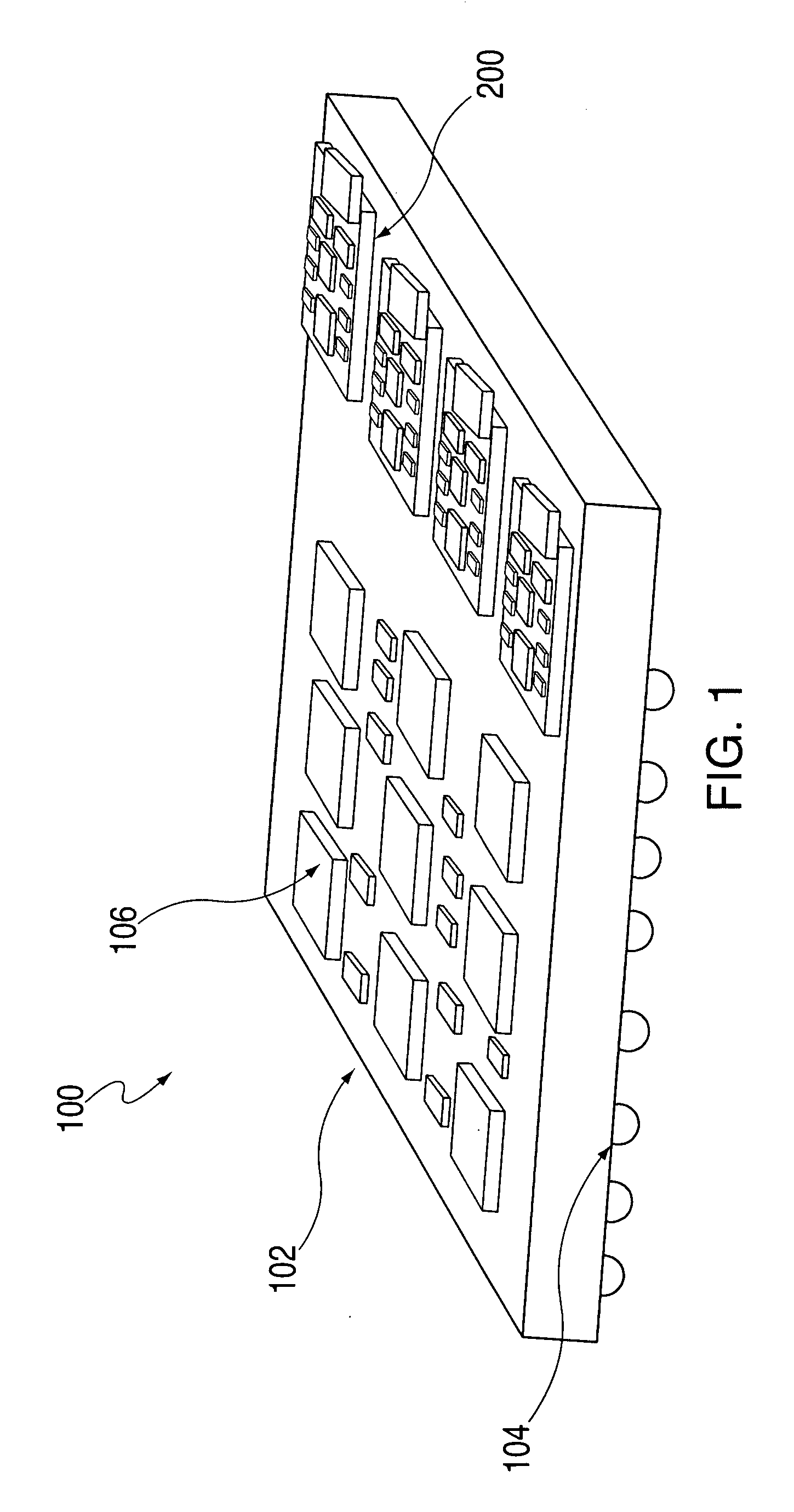
[0009]FIG. 1 is a perspective view of an optical interconnect assembly 100 in an embodiment of the invention. The optical interconnect assembly 100 includes a substrate 102. Substrate 102 may be a multilayer ceramic card, printed circuit board, etc. Interconnects 104 are positioned on the bottom of substrate 102. Although a ball grid array (BGA) is shown in FIG. 1, interconnects 104 may be any known type of electrical and / or optical interconnects.

[0010] The top surface of substrate 102 includes a number of integrated circuits 106. Integrated circuits (ICs) 106 are typically electrical components and coupled to interconnects 104 and / or optical interconnect modules 200 through electrical vias within substrate 102. ICs 106 may provide support functions for the optical interconnect modules 200 and be lower speed (e.g., 5-10 Gb / s) CMOS devices.

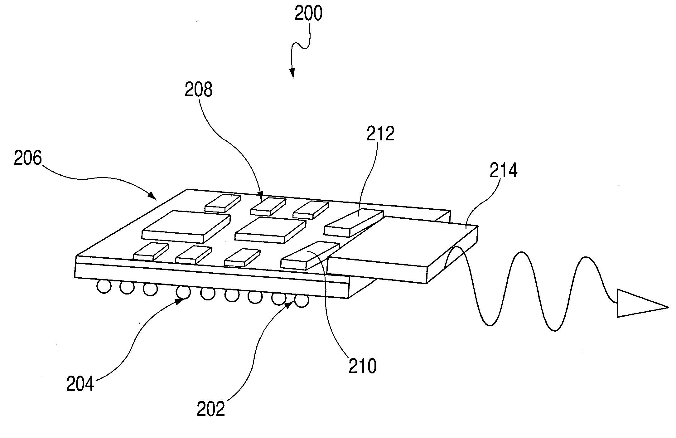
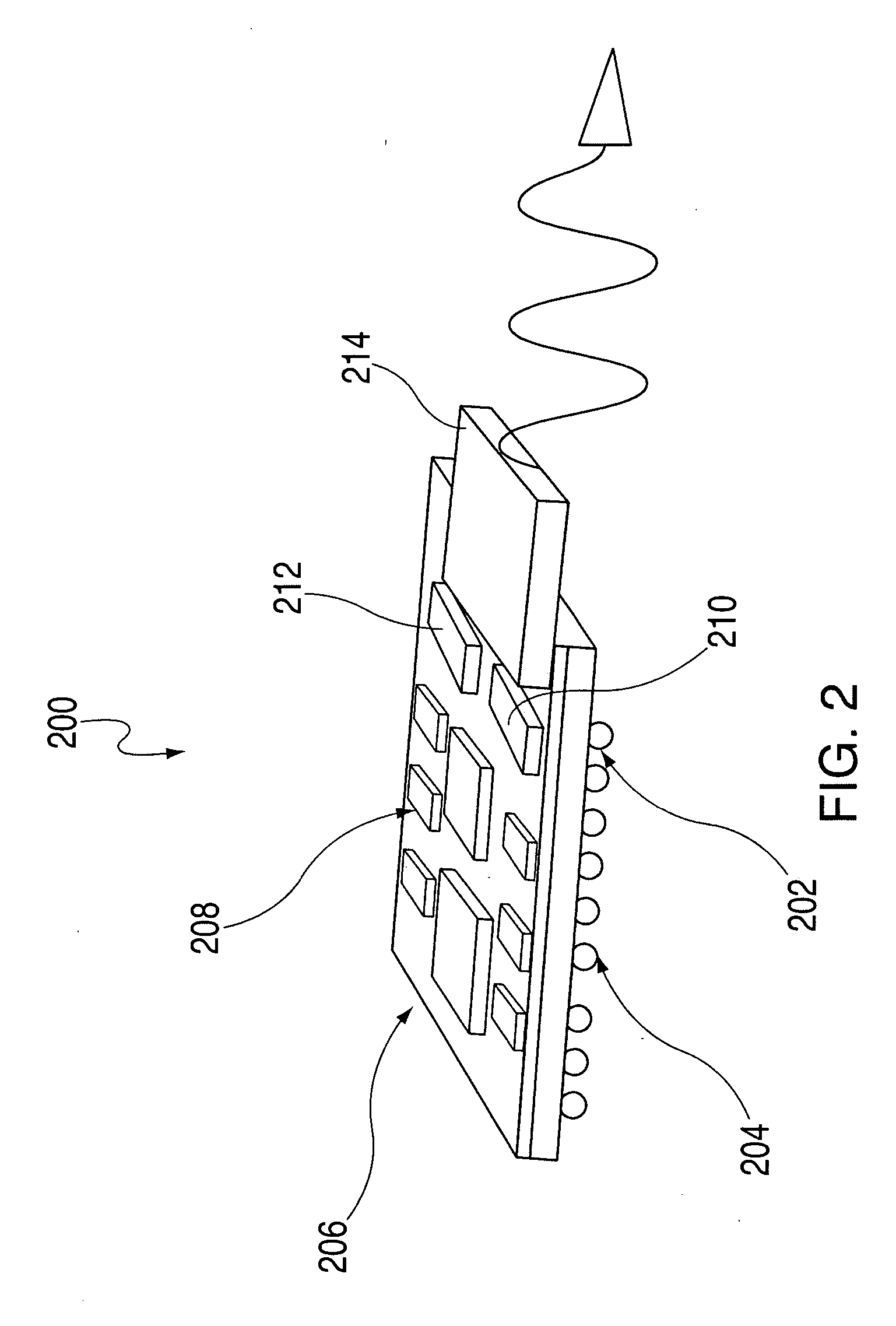
[0011]FIG. 2 is a perspective of optical interconnect module 200 in an embodiment of the invention. Optical interconnect module 200 includes a c...


PUM


Abstract

An embodiment of the invention is an optical interconnect module comprising a silicon carrier; a communication integrated circuit mounted on the silicon carrier and an optical integrated circuit flip chip mounted on the silicon carrier. The optical integrated circuit is in electrical communication with the communication integrated circuit by electrical paths in the silicon carrier. Optical paths in the silicon carrier provide optical coupling between the optical integrated circuit and an optical link.

Description

BACKGROUND OF THE INVENTION [0001] The present disclosure relates generally to optical interconnects and particularly to a silicon carrier for optical interconnect modules. [0002] Optical interconnects are used in a variety of application to couple optical components to electrical components. It is generally recognized that a preferred approach to this problem involves integration of optical components into multichip modules (MCMs) or single chip modules (SCMs). One existing technique includes directly mounting a laser array onto the silicon germanium (SiGe) laser driver chip. This approach, however, adds extra cost and creates difficult thermal challenges. The thermal challenges are twofold; first, the thermally sensitive laser is in intimate contact with the heat producing SiGe driver circuits which affects both laser performance and reliability. Second, a heat spreader on the driver circuit is made significantly less effective, since the contact area to the driver is small becaus...

Claims


Application Information

Patent Timeline
IPC IPC(8): G02B6/00G02B6/12G02B6/26G02B6/42G02B6/43H01S5/022H04B10/02H04B10/12
CPCG02B6/4214G02B6/43G02B6/4232H01L2224/16225H01L2224/73253H01L2924/15311G02B6/428H05K1/0274
Inventor CROW, JOHN D.DECUSATIS, CASIMER M.KASH, JEFFREY A.TREWHELLA, JEAN M.
Owner MARVELL ASIA PTE LTD
Why Eureka
Try Eureka