Method for plasma etching using periodic modulation of gas chemistry

a plasma etching and gas chemistry technology, applied in the direction of basic electric elements, semiconductor/solid-state device manufacturing, electric apparatus, etc., can solve the problems of cd enlargement, pattern distortion, pattern distortion,

Inactive Publication Date: 2005-06-23
LAM RES CORP
View PDF51 Cites 77 Cited by
  • Summary
  • Abstract
  • Description
  • Claims
  • Application Information

AI Technical Summary

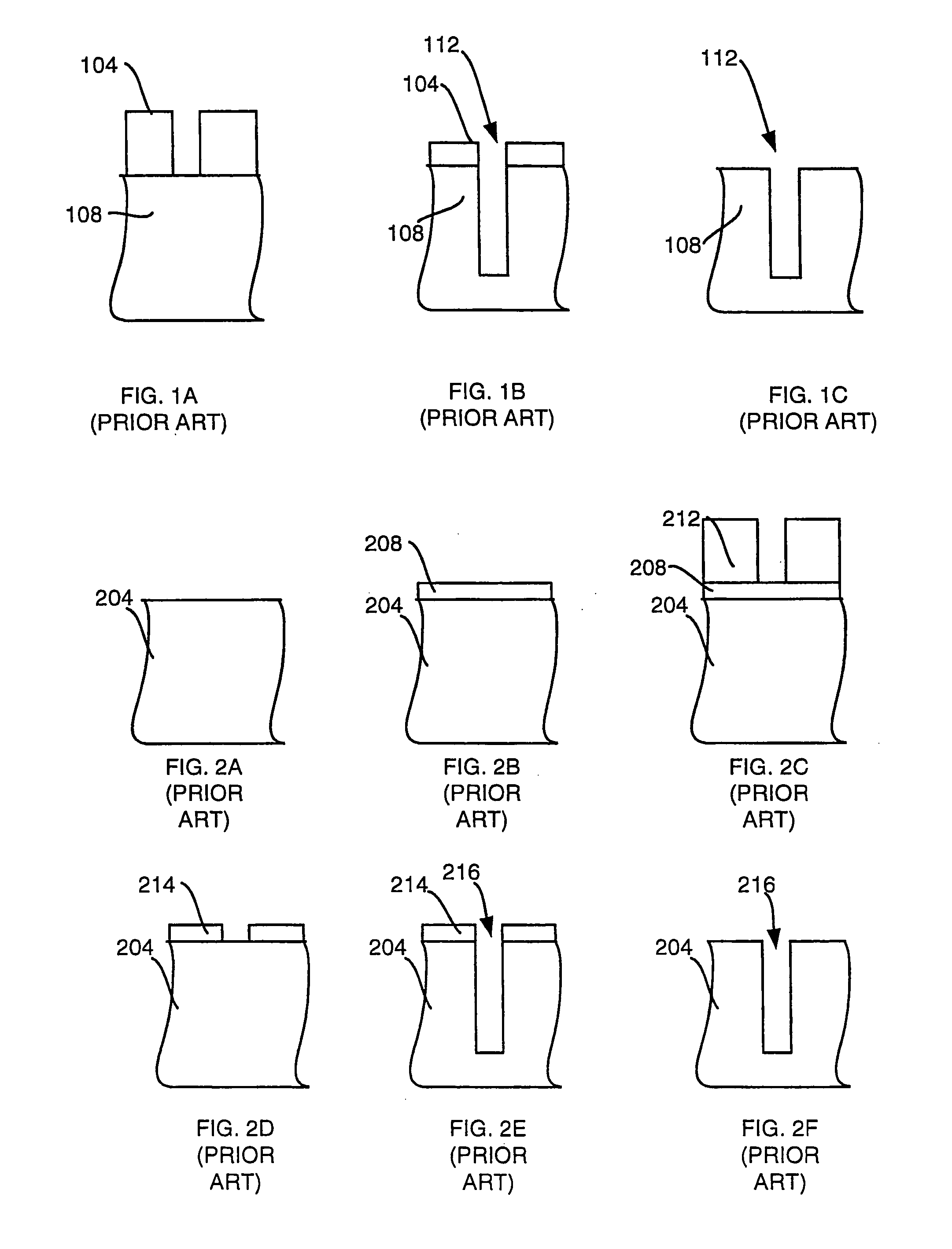
Problems solved by technology

During the etching process, the mask materials are usually eroded and / or damaged in exchange for the pattern transfer.
Consequently, some of the damage and erosion also may be transferred to the underlying layers leaving such undesirable pattern distortions such as striation, CD enlargement, faceting, etc.
A common disadvantage of the above mentioned methods is that the optimum conditions for different aspects of the etching requirement usually do not coincide and by mixing the gases some of the unique properties of each precursor gases may be lost due to inter-reactions.
Additionally, without the passivation gas in the etching mixture, it may be difficult to obtain sufficient etching selectivity to the masking materials if the desire is there to use higher ion energies.
It is also believed that such processes have undesirable striation and faceting.
The disadvantages of this method are that, by introducing new process steps and new tool sets into the process flow, it is of higher cost and lower overall throughput.
In addition, the extra process complexity also introduces difficulties by itself.
For example, the Si hardmask used for dielectric contact etch applications is not as easily stripped as the photoresist mask.

Method used


Image

  • Method for plasma etching using periodic modulation of gas chemistry
  • Method for plasma etching using periodic modulation of gas chemistry
  • Method for plasma etching using periodic modulation of gas chemistry

Examples


example

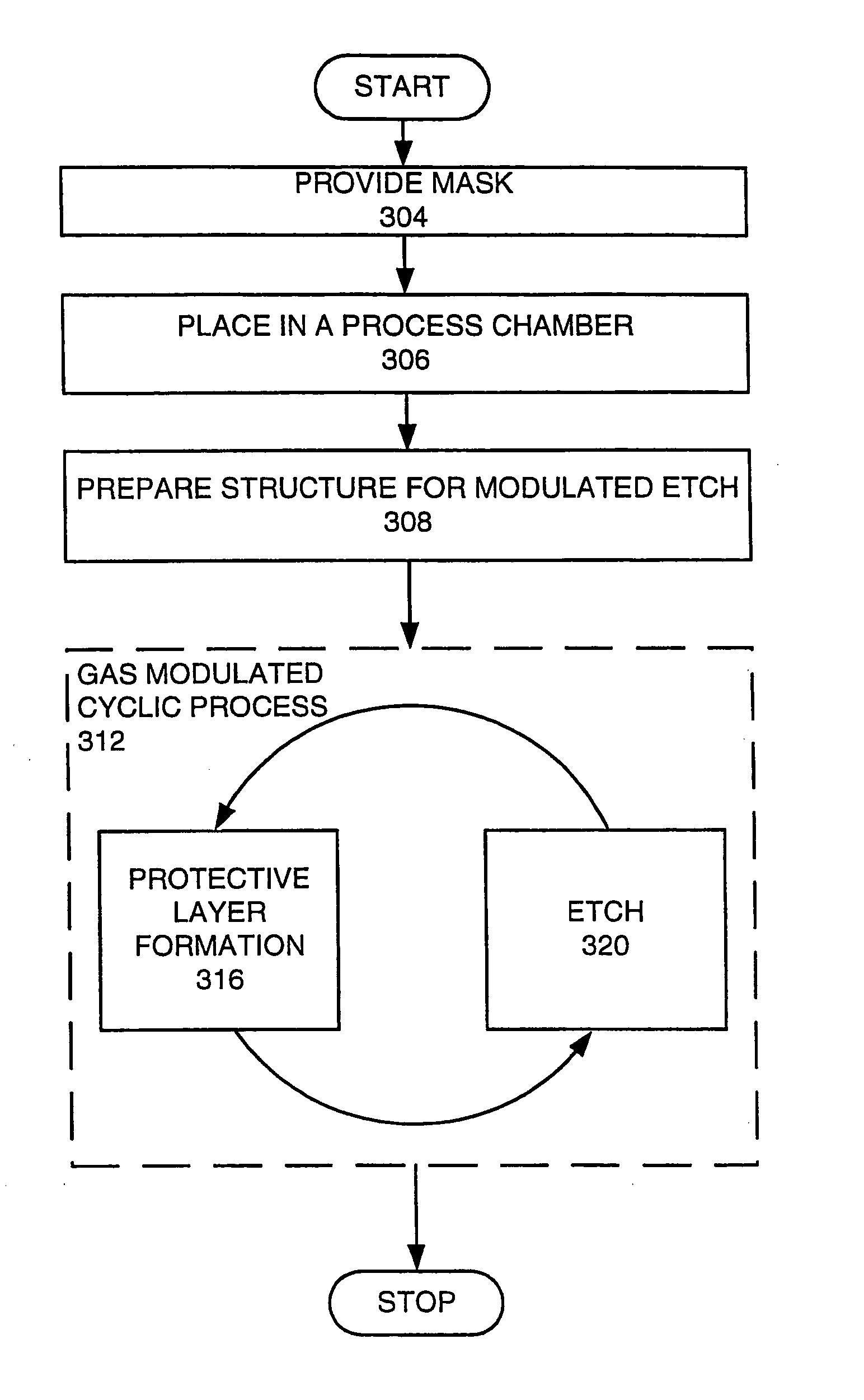
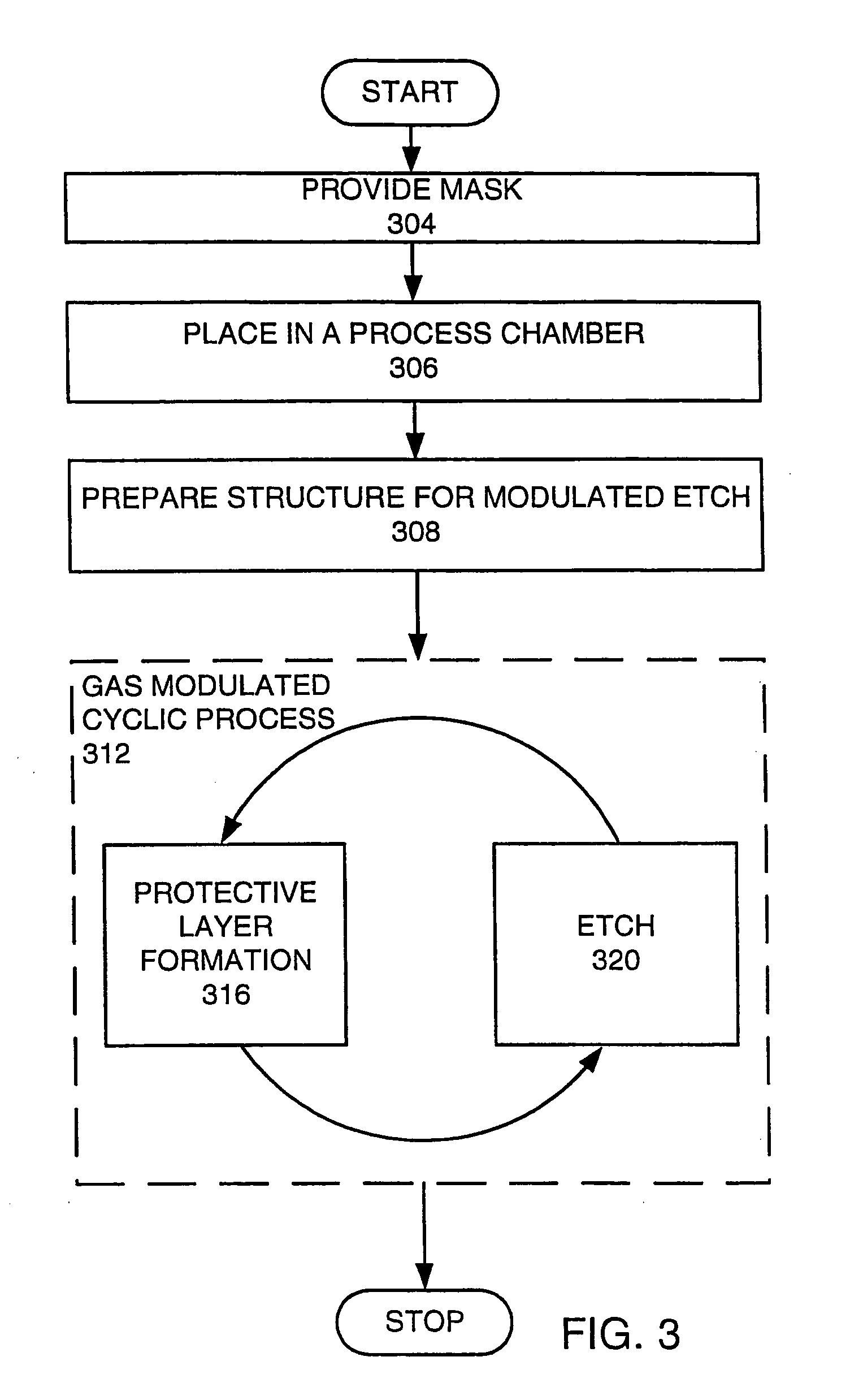
[0079] A specific example of the invention, as applied to etching a HARC structure, uses a Exelang HPT dielectric etch system made by Lam Research Corporation™ of Fremont, Calif. for the process chamber 500. The wafers used in this example include a 2.1 μm SiO2 layer, a patterned photoresist mask, and a bottom antireflective coating (BARC) between the SiO2 layer and the photoresist mask. The SiO2 layer used in this example is deposited using plasma enhanced CVD with a tetraethylorthosilicate (TEOS) precursor. The photoresist mask is patterned using 193 nm photolithography, to produce a contact critical dimension (CD) of 0.16 μm or less.

[0080] In this example the preparation of the structure (step 306) for the gas-modulated cyclic etch is a BARC etch step. In this example the BARC etch step may one of many known BARC etch steps.

[0081] Upon completion of the BARC etch step, the cyclic process is performed in the Exelan HPT dielectric etch system. In this example, which uses an Exela...


PUM


Abstract

A method for etching a layer over a substrate is provided. A gas-modulated cyclic process is performed for more than three cycles. Each cycle comprises performing a protective layer forming phase using first gas chemistry with a deposition gas chemistry, which is performed in about 0.0055 to 7 seconds for each cycle and performing an etching phase for the feature through the etch mask using a second gas chemistry using a reactive etching gas chemistry, which is performed in about 0.005 to 14 seconds for each cycle. The protective layer forming phase comprises providing the deposition gas and forming a plasma from the deposition gas. Each etching phase comprises providing a reactive etching gas and forming a plasma from the reactive etching gas.

Description

BACKGROUND OF THE INVENTION [0001] 1. Field of the Invention [0002] The invention relates to a method of obtaining a structure on a semiconductor wafer by etching through structures defined by a mask, such as a photoresist mask, hard mask, or a stacked mask, using a plasma. [0003] 2. Description of the Related Art [0004] In semiconductor plasma etching applications, a plasma etcher is usually used to transfer a mask pattern into a circuit and line pattern of a desired thin film and / or filmstack (conductors or dielectric insulators) on a wafer. This is achieved by etching away the films (and filmstacks) underneath the photoresist materials in the opened areas of the mask pattern. This etching reaction may be initiated by the chemically active species and electrically charged particles (ions) generated by exciting an electric discharge in a reactant mixture contained in a vacuum enclosure also referred to as a reactor or process chamber. Additionally, the ions may be also accelerated ...

Claims


Application Information

Patent Timeline
Patent Type & Authority Applications(United States)
IPC IPC(8): H01L21/302H01L21/3065H01L21/461
CPCH01L21/31116H01L21/30655H01L21/302H01L21/3065
Inventor HUDSON, ERIC A.TIETZ, JAMES V.
Owner LAM RES CORP
Why Eureka
Try Eureka