High power light emitting diode package and fabrication method thereof

a technology of light-emitting diodes and led packages, which is applied in the manufacture of semiconductor/solid-state devices, electrical apparatus, and semiconductor devices. it can solve the problems of high defect rate of assembly/connection process, large overall package size, and difficult fabrication of high-power led packages

Inactive Publication Date: 2005-06-30
SAMSUNG ELECTRO MECHANICS CO LTD
View PDF7 Cites 208 Cited by
  • Summary
  • Abstract
  • Description
  • Claims
  • Application Information

AI Technical Summary

Benefits of technology

[0027] As set forth above, the present invention proposes an approach of mounting the LED via flip chip bonding instead of wire bonding that is a main factor causing a complicated structure and assembly process as well as defects. Further, the present invention provides a novel structure capable of enhancing heat radiation effect while utilizing flip chip bonding LED.

Problems solved by technology

Fabrication of the high power LED package is difficult owing to a complicated process such as a die bonding and a wire bonding of the LED.
In particular, its assembly / connection process such as wire bonding may have a high percent defective, and the wires may act as a factor for increasing the size of the overall package.
More particularly, although the package shown in FIG. 2a may also have a plurality of conductive via holes (not shown) formed in the lower ceramic board 11 to promote heat radiation from the LED 15, the size and number of the conductive via holes is essentially restricted to stably support an LED chip while preventing unwanted contact with the lead frames As a consequence, the LED package has a relatively lower heat radiation effect than that of the package in FIG. 1a, and thus cannot sufficiently endure the heat generated from the high power LED.
As described above, the conventional LED package tends to be defective owing to its complicated structure and fabrication process.
To the contrary, the package of a simple structure has a problem that heat radiation effect, which is one of its major functions, is degraded.

Method used


Image

  • High power light emitting diode package and fabrication method thereof
  • High power light emitting diode package and fabrication method thereof
  • High power light emitting diode package and fabrication method thereof

Examples


Embodiment Construction

[0036] Preferred embodiments of the present invention will now be described in detail with reference to the accompanying drawings.

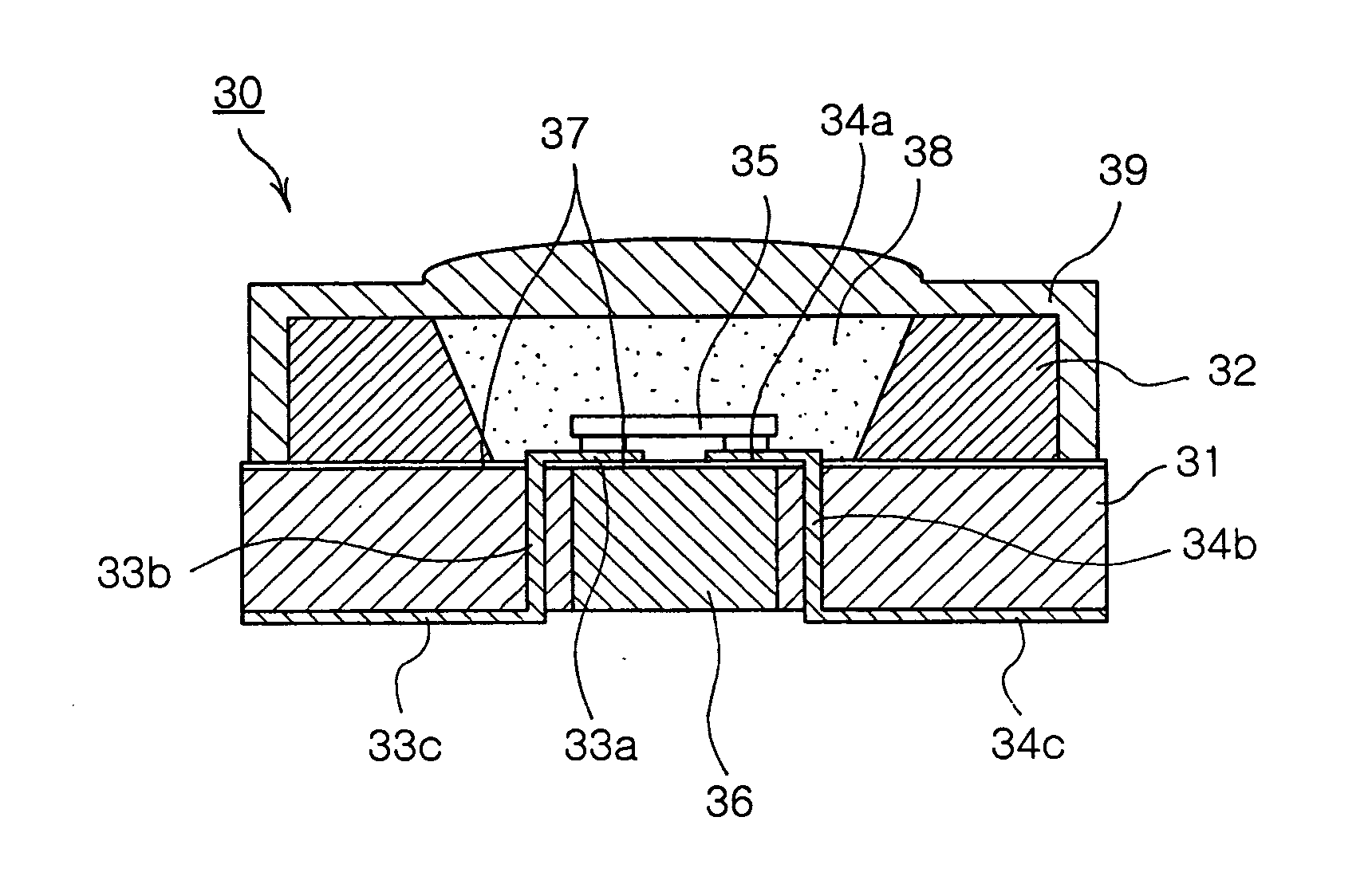
[0037]FIG. 3 is a sectional view illustrating a high power LED package according to a preferred embodiment of the invention.

[0038] Referring to FIG. 3, a high power LED package 30 includes a lower board 31 mounted with an LED 35 and an upper board 32 surrounding an area where the LED 35 is arranged.

[0039] The lower board 31 includes a heat radiation member 36 formed in a substantially central area and first and second conductive via holes 33b and 34b defining two vertical connection structures. Unlike the conductive via holes 33b and 34b of tens μm sizes, the heat radiation member 36 has a size corresponding to the that of the LED 35. The heat radiation member 36 can be made by filling conductive material into a cavity of a sufficient size formed in the lower board 31. The heat radiation member 36 has a sectional area preferably matching about 50% of t...


PUM


Abstract

Disclosed is a high power LED package. In the LED package, a lower board has a heat radiation member in an LED mounting area and at least one via hole around the heat radiation member. First and second bottom electrodes are formed in the underside of the lower board, and connected to the heat radiation member and the via hole. An insulation layer is formed on the lower board to cover the heat radiation member. First and second electrode patterns on the insulation layer are connected to the first and second bottom electrodes through the via hole.

Description

BACKGROUND OF THE INVENTION [0001] 1. Field of the Invention [0002] The present invention relates to a light emitting diode package, and more particularly, a high power light emitting diode package which can enhance heat radiation effect as well as omit a wire bonding procedure to simplify a package structure and reduce the package size. [0003] 2. Description of the Related Art [0004] Light Emitting Diodes (LEDs) are widely used owing to several advantages such as low power consumption and high brightness, and in particular, recently utilized in illumination devices and as backlights for large-sized Liquid Crystal Displays (LCDs). The LEDs are provided in the form of packages to be easily mounted on the illumination devices and so on. LED protection ability, connection structures to main devices and heat radiation performance for radiating heat generated from LEDs are main bench-marks of the LED packages. High heat radiation performance is a more important package requirement in an ...

Claims


Application Information

Patent Timeline
Patent Type & Authority Applications(United States)
IPC IPC(8): H01L33/44H01L21/00H01L33/56H01L33/58H01L33/60H01L33/62H01L33/64
CPCH01L33/486H01L33/62H01L33/642H01L33/647H01L2224/16H01L2224/48091H01L2224/48247H01L2924/01078H01L2924/09701H01L2224/48227H01L2924/12041H01L2924/00014
Inventor PARK, JUNG KYUPARK, CHAN WANGYOON, JOON HOKIM, CHANG WOOKPARK, YOUNG SAM
Owner SAMSUNG ELECTRO MECHANICS CO LTD
Why Eureka
Try Eureka