Method and device for manufacturing bonding pads for chip scale packaging

a technology of chip scale and bonding pads, which is applied in the direction of semiconductor devices, semiconductor/solid-state device details, electrical equipment, etc., can solve the problems of reducing the yield of chips, and reducing the cost of integrated circuit or chip fabrication facilities, so as to improve the bump structure, improve the yield, and facilitate the use

Inactive Publication Date: 2005-06-30
SEMICON MFG INT (SHANGHAI) CORP
View PDF8 Cites 16 Cited by
  • Summary
  • Abstract
  • Description
  • Claims
  • Application Information

AI Technical Summary

Benefits of technology

[0009] Many benefits are achieved by way of the present invention over conventional techniques. For example, the present technique provides an easy to use process that relies upon conventional technology. In some embodiments, the method provides higher device yields in packaged dies. Additionally, the method provides a process that is compatible with conventional process technology without subst

Problems solved by technology

An integrated circuit or chip fabrication facility can cost hundreds of millions, or even billions, of U.S. dollars.
Making devices smaller is very challenging, as each process used in integrated fabrication has a limit.
Additionally, as devices require fast

Method used


Image

  • Method and device for manufacturing bonding pads for chip scale packaging
  • Method and device for manufacturing bonding pads for chip scale packaging
  • Method and device for manufacturing bonding pads for chip scale packaging

Examples


Embodiment Construction

[0014] According to the present invention, techniques for packaging integrated circuits for the manufacture of semiconductor devices are provided. More particularly, the invention provides a method for manufacturing a contact structure for packaging advanced integrated circuits such as microprocessors, application specific integrated circuits, memories, mixed signal applications, and the like. But it would be recognized that the invention has a much broader range of applicability.

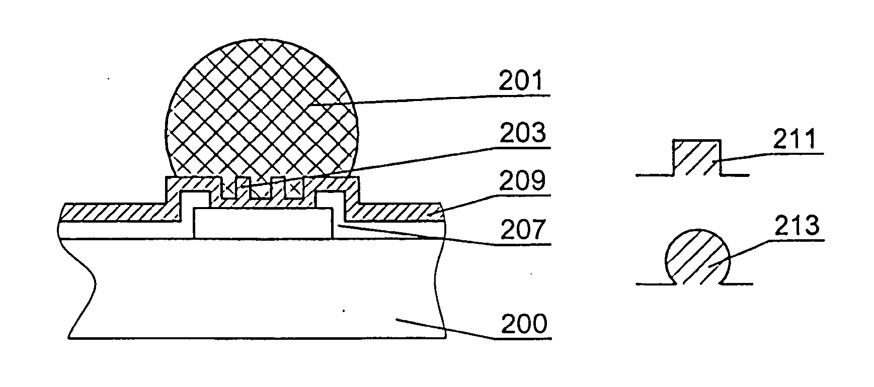
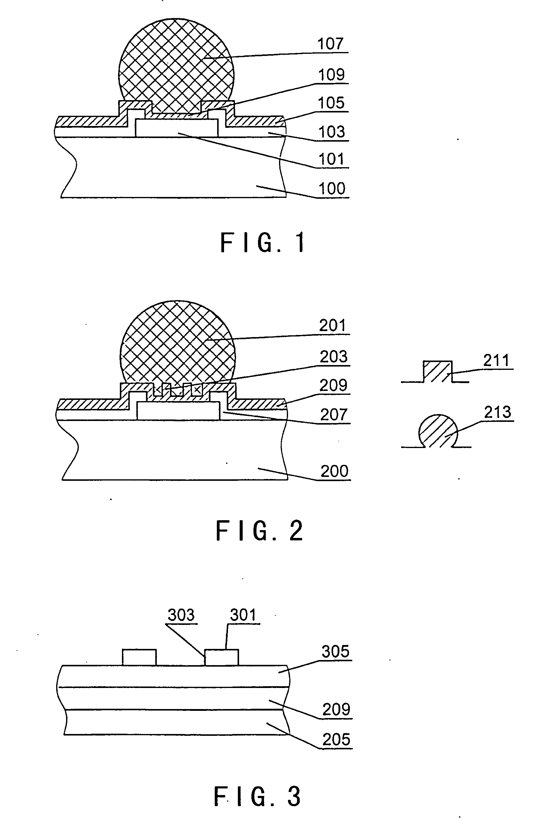
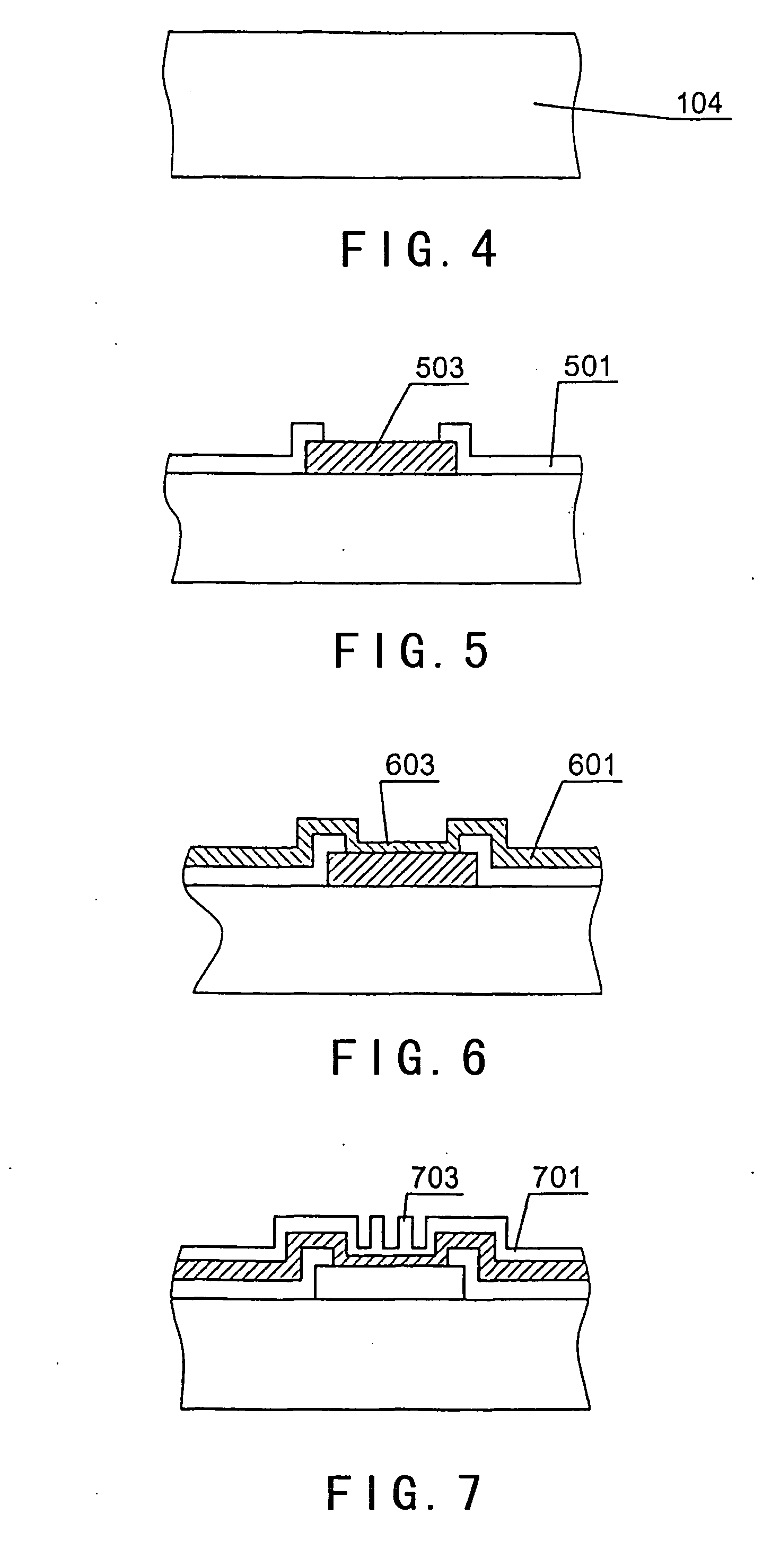
[0015]FIG. 1 is a simplified cross-sectional view diagram of an interconnect structure of conventional devices. As shown, the conventional device includes a substrate 100. A bonding pad 101 is disposed on the substrate. A passivation layer 103 overlies the substrate while maintaining an opening over a portion of the bonding pad. The structure also has an overlying UBM layer 105, which has a smooth surface overlying the bond pad. A bump layer 107 is formed overlying the UDP layer. Many limitations exist wit...


PUM


Abstract

An integrated circuit chip and method of manufacture. The chip has a substrate, e.g., silicon, silicon on insulator, epitaxial wafer. The substrate has a plurality of chip structures. A plurality of bonding pads are disposed on the substrate. Each of the bonding pads is formed from an aluminum bearing material or other like material. A surface region is formed on each of the bonding pads. An under bump metal layer (“UBM”) is overlying the surface region. A wetting layer is formed overlying the under bump metal layer. The wetting layer comprises a plurality of protrusions extending out of the wetting layer and disposed spatially on the wetting layer. A bump layer is formed overlying the wetting layer and is mechanically coupling to the plurality of protrusions.

Description

BACKGROUND OF THE INVENTION [0001] The present invention is directed to integrated circuits and their packaging for the manufacture of semiconductor devices. More particularly, the invention provides a method for manufacturing a contact structure for packaging advanced integrated circuits such as microprocessors, application specific integrated circuits, memories, mixed signal applications, and the like. But it would be recognized that the invention has a much broader range of applicability. [0002] Integrated circuits have evolved from a handful of interconnected devices fabricated on a single chip of silicon to millions of devices. Conventional integrated circuits provide performance and complexity far beyond what was originally imagined. In order to achieve improvements in complexity and circuit density (i.e., the number of devices capable of being parked onto a given chip area), the size of the smallest device feature, also known as the device “geometry”, has become smaller with ...

Claims


Application Information

Patent Timeline
IPC IPC(8): H01L21/60H01L23/485
CPCH01L24/03H01L24/05H01L24/13H01L2224/0401H01L2224/05557H01L2224/05558H01L2224/13H01L2224/13099H01L2924/01013H01L2924/01014H01L2924/01022H01L2924/01024H01L2924/01028H01L2924/01029H01L2924/01033H01L2924/01042H01L2924/01078H01L2924/01079H01L2924/014H01L2924/14H01L2924/3011H01L2924/00H01L24/02H01L24/10H01L24/11
Inventor FAN, YUAN-HENG
Owner SEMICON MFG INT (SHANGHAI) CORP
Why Eureka
Try Eureka