Film bulk acoustic wave resonator device and manufacturing method thereof

a technology of acoustic wave resonators and film, which is applied in the direction of piezoelectric/electrostrictive/magnetostrictive devices, piezoelectric/electrostriction/magnetostriction machines, etc., can solve the problem of disadvantageous variation in the resonant frequency of fbar devices, and the frequency variation problem of fbar devices, especially, may be increased, so as to achieve stable protection of the resonance unit

Inactive Publication Date: 2005-06-30
SAMSUNG ELECTRO MECHANICS CO LTD
View PDF3 Cites 52 Cited by
  • Summary
  • Abstract
  • Description
  • Claims
  • Application Information

AI Technical Summary

Benefits of technology

[0013] Therefore, the present invention has been made in view of the above problems, and it is an object of the present invention to provide an FBAR device, which can achieve appropriate adjustment in a resonant frequency thereof and stable protection of its resonance unit during a subsequent process. This objective is accomplished by virtue of a passivation layer formed substantially throughout the resonance unit, rather than being formed only on an upper electrode of the resonance unit.
[0014] It is another object of the present invention to provide an FBAR device, and a method of manufacturing an FBAR device package, which shows additional advantages in relation to the formation of a cap structure in a chip scale packaging or wafer level packaging process.
[0018] In general, the FBAR device is basically classified into an air gap manner device and a bragg reflection manner device according to an insulation structure between the substrate and a resonance unit, and the present invention can be effectively applied into both the devices. Therefore, the substrate may include an air gap formed at a region where the resonance unit is formed thereabove. Alternatively, the substrate may have a reflective film structure obtained through bragg reflection.
[0023] Preferably, the step d-2) and the step f) may be simultaneously performed through a single process using a photoresist film, the sacrificial material region may be made of a polysilicon material, the step g) may be an etching step of the sacrificial material region using XeF2. Advantageously, in the step g), the passivation layer may protect the upper electrode.
[0024] In accordance with yet another aspect of the present invention, the above and other objects can be accomplished by the provision of a method of manufacturing an FBAR device package comprising the steps of: a) preparing a substrate; b) forming a resonance unit by successively stacking a lower electrode, a piezoelectric film, and an upper electrode on the substrate; c) calculating a thickness of the resonance unit required to compensate for a difference between a resonant frequency of the resonance unit and a desired target resonant frequency; d) forming a passivation layer substantially throughout an upper surface and peripheral surface of the resonance unit for protecting the resonance unit so that a partial region of the passivation layer located on at least the upper electrode has the calculated thickness; and e) forming a cap structure so as to seal the resonance unit formed with the passivation layer.

Problems solved by technology

With the present technical level, however, it is substantially impossible to make respective FBAR devices in a wafer to have the same thickness as each other within a tolerance range of approximately 1 percent of the thickness.
Moreover, the upper electrode made of metal tends to cause an oxidation phenomenon thereof, resulting in disadvantageous variation in the resonant frequency of the FBAR device.
Such a frequency variation problem of the FBAR device, especially, may be increased during a packaging process due to oxidation.
This solution, however, still exhibits an oxidation problem of the upper metal electrode during a subsequent process.
The above described conventional FBAR device 10, however, has a problem in that there is a limitation of the thickness of the thermal oxide film 18 obtainable through the thermal oxidation process, resulting in a considerable restriction in adjustable frequency range.
In view of frequency stabilization, further, the presence of the thermal oxide film 18 only affects to delay an oxidation speed of the upper electrode made of metal during a subsequent process, and thus it is difficult to completely prevent an actual oxidation progress itself.
Furthermore, since the thermal oxide film 18 formed on the upper electrode 16 tends to be damaged in a subsequent process, especially, in the manufacture of a package accompanying with a photoresist process or slicing process, there may be a risk of an unintentional sudden frequency variation.

Method used


Image

  • Film bulk acoustic wave resonator device and manufacturing method thereof
  • Film bulk acoustic wave resonator device and manufacturing method thereof
  • Film bulk acoustic wave resonator device and manufacturing method thereof

Examples


Embodiment Construction

[0031] Now, the present invention will be described, with reference to the accompanying drawings.

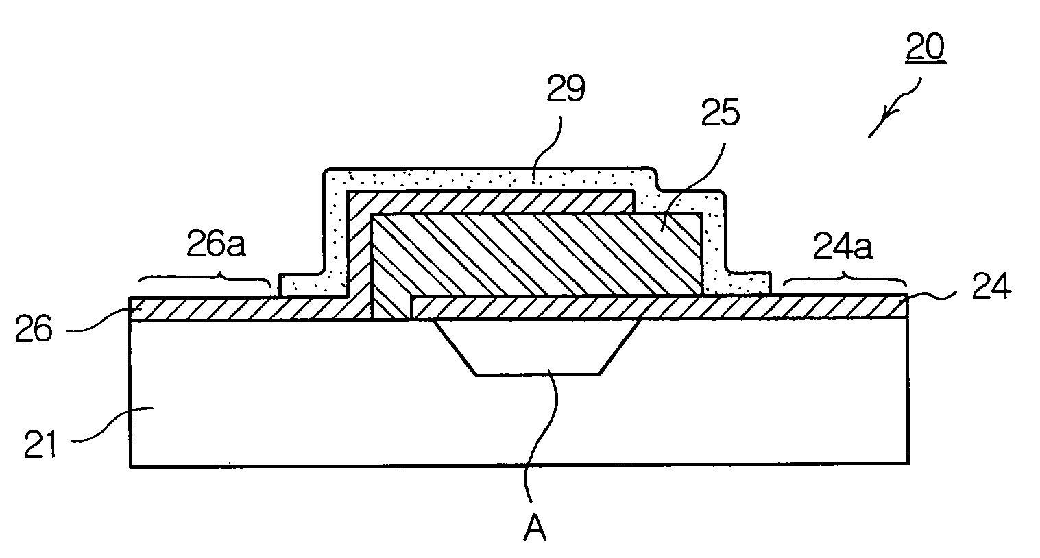
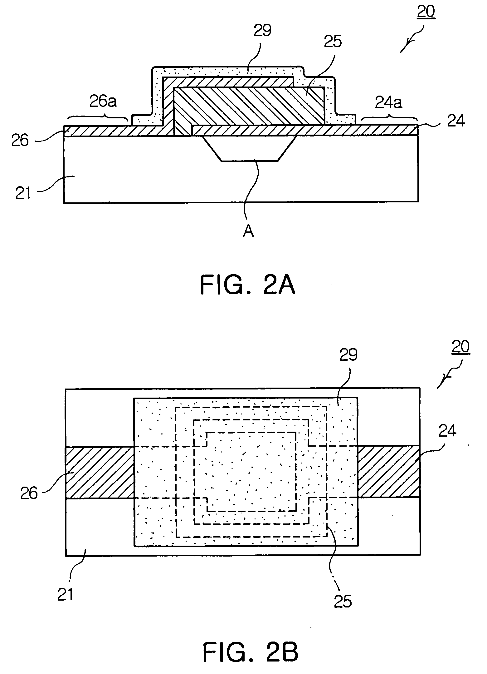
[0032]FIGS. 2a and 2b are a side sectional view and a plan view, respectively, illustrating an FBAR device in accordance with an embodiment of the present invention.

[0033] Referring to FIG. 2b along with FIG. 2a, the FBAR device of the present invention, designated as reference numeral 20, comprises a substrate 21 formed at an upper surface thereof with a resonance unit. The resonance unit comprises a lower electrode 24, a piezoelectric layer 25, and an upper electrode 26, which are successively stacked on the substrate 21 so that they are positioned above an air gap (A) defined in the substrate 21. Mainly, the substrate 21 may be a silicon substrate, the upper and lower electrodes 26 and 24 may be made of molybdenum (Mo), and the piezoelectric layer 25 may be made of aluminum nitride (AlN), but are not limited thereto.

[0034] The FBAR device 20 in accordance with the present invention...


PUM


Abstract

Disclosed herein is an FBAR (film bulk acoustic wave resonator) device and a manufacturing method thereof. The FBAR device comprises a substrate, a resonance unit including a lower electrode, a piezoelectric film, and an upper electrode, which are successively stacked on the substrate, and a passivation layer formed substantially throughout an upper surface and peripheral surface of the resonance unit in order to protect the resonance unit. A partial region of the passivation layer formed on at least the upper electrode has a thickness required to compensate for a difference between a resonant frequency of the resonance unit and a desired target resonant frequency.

Description

BACKGROUND OF THE INVENTION [0001] 1. Field of the Invention [0002] The present invention relates to a film bulk acoustic wave resonator (hereinafter, referred to as an FBAR), and more particularly to an FBAR device and a manufacturing method thereof, which can achieve ease of frequency adjustment, and minimize a risk in generation of poor products during a packaging process. [0003] 2. Description of the Related Art [0004] According to the recent trend wherein mobile communication terminals have tended to become much leaner and enhanced and diversified in their quality and functions, techniques related with constituent components of the mobile communication terminals, for example radio frequency (RF) components, are rapidly being developed. Among the RF components, especially, an FBAR (film bulk acoustic wave resonator) is in the spotlight as an essential passive filter component of the mobile communication terminals by virtue of its advantages in that it has a lower insertion loss ...

Claims


Application Information

Patent Timeline
Patent Type & Authority Applications(United States)
IPC IPC(8): H01L41/08H01L41/09H01L41/22H01L41/23H01L41/253H01L41/29H03H3/02H03H3/04H03H9/02H03H9/10H03H9/17H03H9/24
CPCH03H3/04H03H9/173H03H9/105H03H9/02149H03H9/24
Inventor LEE, JOO HO
Owner SAMSUNG ELECTRO MECHANICS CO LTD
Why Eureka
Try Eureka