Probe navigation method and device and defect inspection device

Active Publication Date: 2005-06-30
HITACHI HIGH-TECH CORP
View PDF3 Cites 18 Cited by
  • Summary
  • Abstract
  • Description
  • Claims
  • Application Information

AI Technical Summary

Benefits of technology

[0009] Recently, wiring patterns formed on semiconductor wafers have been increasingly microminiaturized. The positioning accuracy demanded in probing is presently on the order of nm. It is difficult to automatize probing with such high accuracy with the present technology, and there is no other choice but to manually perform probing operation. Further, the size of wafers used in the manufacturing processes for semiconductor devices has been increased as compared with conventional wafers. This increases a burden on equipment users during pro

Problems solved by technology

It is difficult to automatize probing with such high accuracy with the present technology, and there is no other choice but to manually perform probing operation.
This increases a burden on equipment users during probing operation.
However, it cannot be said that the conventional equipmen

Method used


Image

  • Probe navigation method and device and defect inspection device
  • Probe navigation method and device and defect inspection device
  • Probe navigation method and device and defect inspection device

Examples


Example

First Embodiment

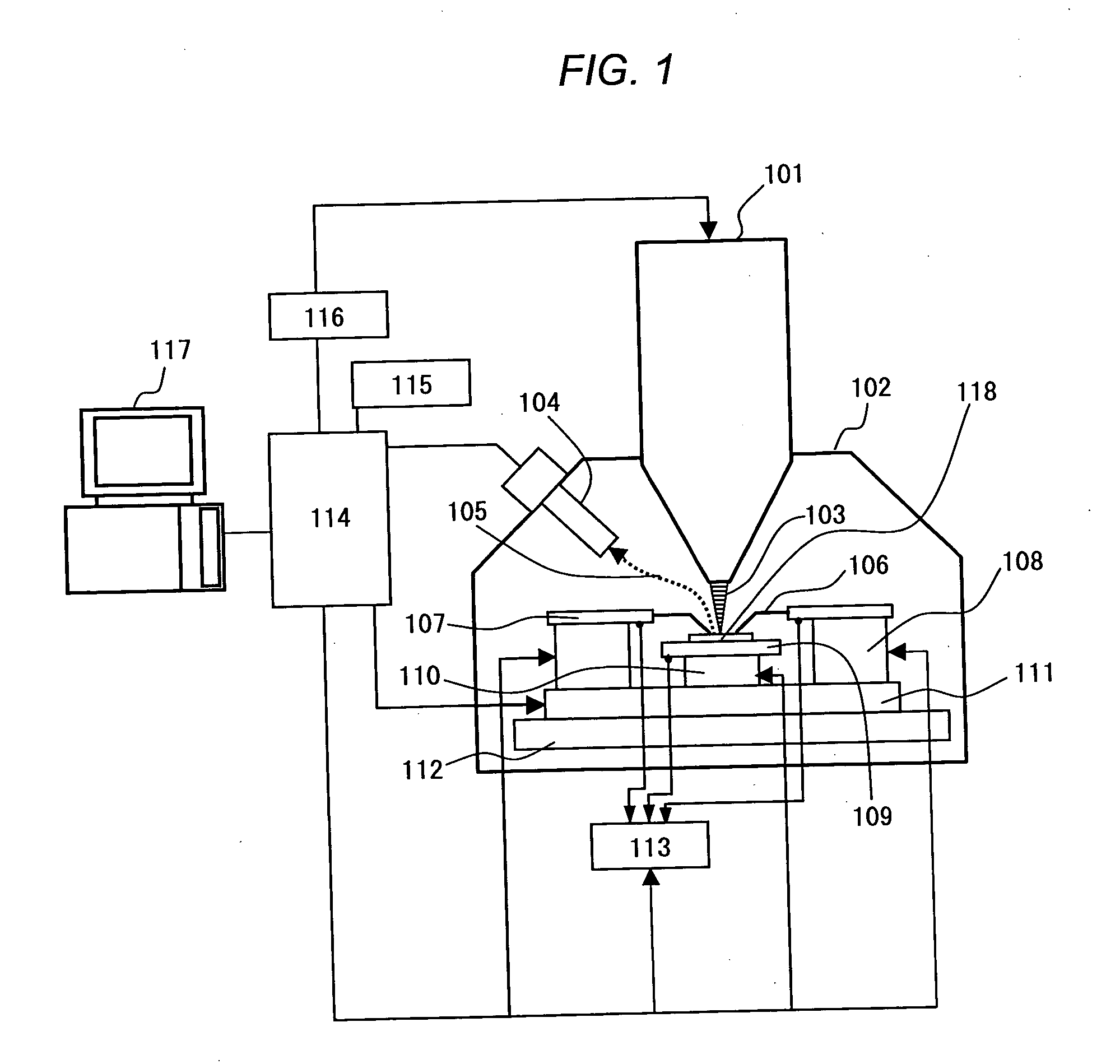
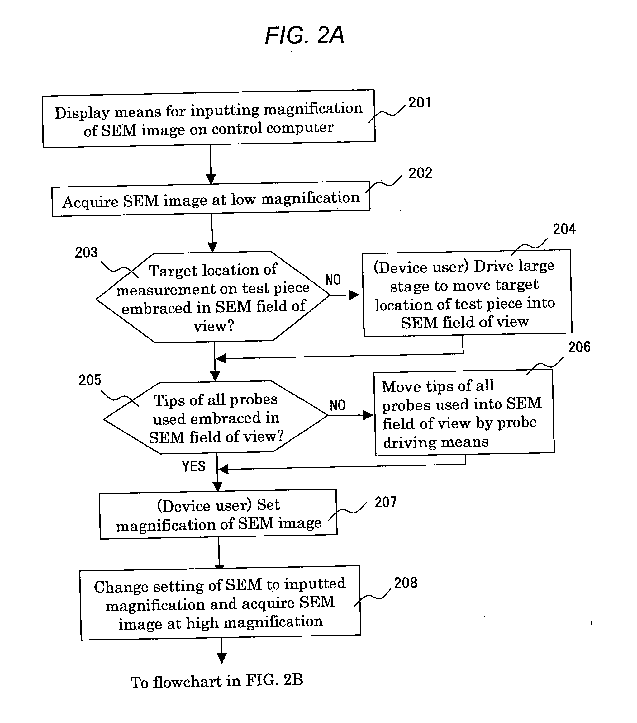
[0028] Description will be given to a first embodiment which involves a defect inspection device with mechanical probes for electrical characteristics evaluation incorporated into the test piece chamber of SEM. FIG. 1 illustrates an example of the configuration of a defect inspection device in which a probe navigation method of the first embodiment is implemented. FIGS. 2A to 2D illustrate the basic flow of inspection carried out using the inspection device of the first embodiment. First, the configuration of the inspection device will be described referring to FIG. 1.

[0029] An electron gun 101 constitutes an irradiation optical system for irradiating a test piece 118 with a primary electron beam 103 and scanning it. Therefore, the electron gun 101 in the first embodiment means a system including all the constituent elements required for electron beam irradiation. Such constituent elements include an electron source which generates an electron beam, and a deflector...

Example

Second Embodiment

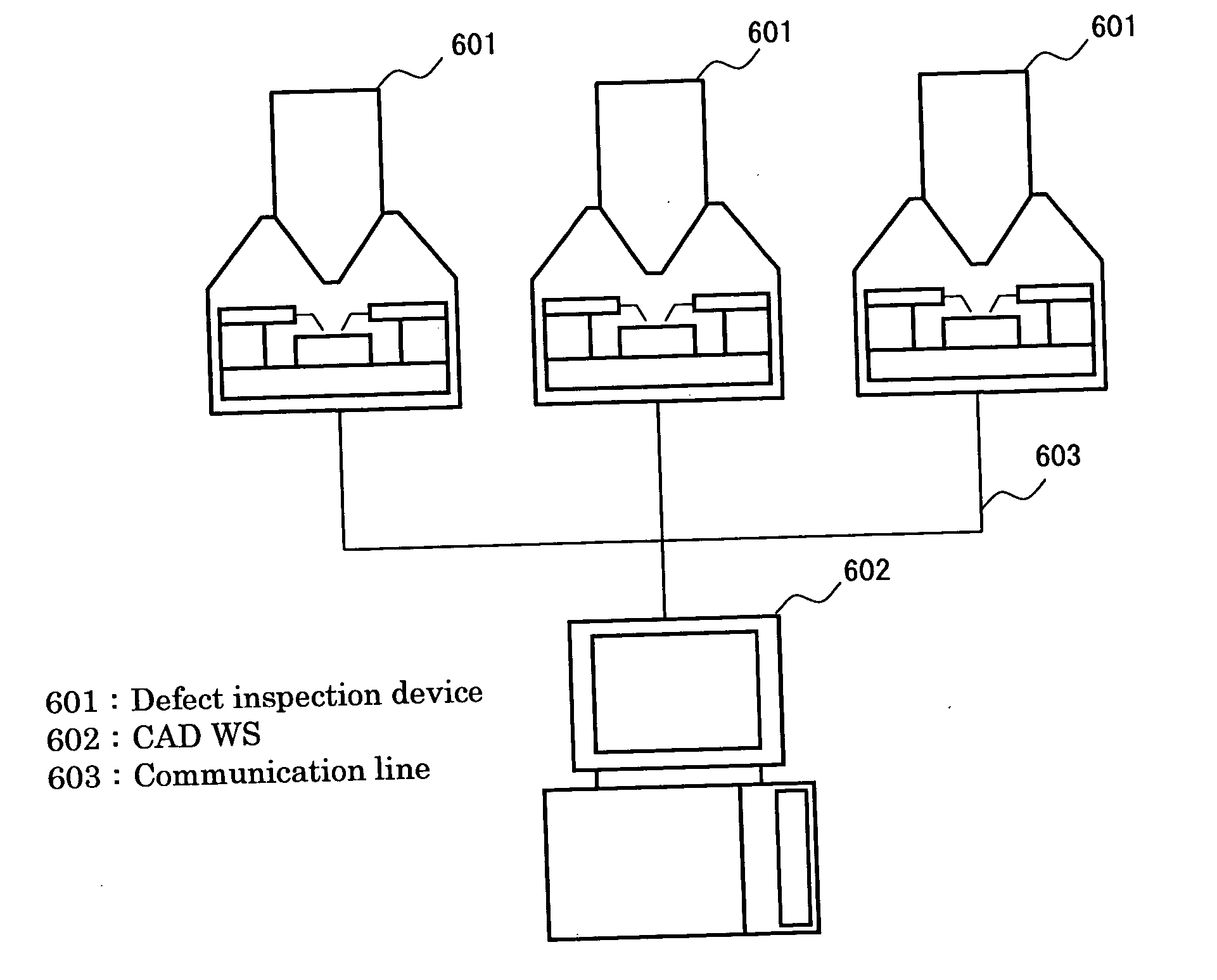
[0060] Description will be given to a second embodiment which involves a defect inspection system so constituted that CAD WS is shared among a plurality of defect inspection devices or failure analyzers. FIG. 6 schematically illustrates a defect inspection system. A plurality of (three) defect inspection devices 601 are connected to CAD WS 602 through communication lines 603. The second embodiment is on the assumption that the internal structure of the three defect inspection devices is the same as the defect inspection device illustrated in FIG. 1. However, any other equipment may be used for this purpose. The three units may be constituted as a combined defect analyzing system comprising a defect inspection device and a failure analyzer. For example, the following combination is acceptable: one of the three units is a defect inspection device illustrated in FIG. 1, and the other two units are a focused ion beam system and a transmission electron microscope. In ca...

Example

Third Embodiment

[0062] Description will be given to a third embodiment. This is another example of the defect inspection device in which mechanical probes for electrical characteristics evaluation are mounted inside the test piece chamber of SEM. FIG. 7 illustrates an example of the configuration of a defect inspection device in which the probe navigation method of the third embodiment is carried out. This configuration is substantially the same as the configuration of the defect inspection device of the first embodiment, illustrated in FIG. 1. Therefore, description will be given only to a difference between them.

[0063] The difference between the device in FIG. 1 and that in FIG. 7 is the presence of an insulating plate 701. The insulating plate 701 is mounted so that it is sandwiched between the test piece stage 109 and the test piece stage driving means 110. Thus, test pieces are electrically insulated from the vacuum chamber partition wall 102, test piece stage driving means 1...


PUM


Abstract

A probe navigation method, a navigation device, and a defect inspection device wherein in a charged particle beam system provided with probes for electrical characteristics evaluation, probing can be easily carried out regardless of the equipment user's level of skill are provided. To attain this object, probes and a test piece stage on which a test piece is placed are driven by independent driving means. Further, a large stage driving means which integrally drives the probes and the test piece stage is provided. In addition, CAD navigation is adopted. This enhances the equipment users' convenience during probing.

Description

CLAIM OF PRIORITY [0001] The present application claims priority from Japanese applications JP 2003-426169 filed on Dec. 24, 2003 and JP 2004-297115 filed on Oct. 12, 2004, the contents of which are hereby incorporated by reference into this application. FIELD OF THE INVENTION [0002] The present invention relates to a method for positioning probes in a defect inspection device which measures the electrical characteristics of electronic devices using the minute probes, and to a defect inspection device using the positioning method. BACKGROUND OF THE INVENTION [0003] Varied inspection equipment is conventionally known for detecting electrical defects in minute electronic circuits formed on a semiconductor chip. Such inspection equipment includes EB tester (Electron Beam tester) and prober device. The EB tester is a device for detecting points of electrical defect in LSIs. This detection is carried out by irradiating a point of measurement with an electron beam utilizing the following ...

Claims


Application Information

Patent Timeline
IPC IPC(8): G01R31/302G01R31/28G01R31/307H01L21/66
CPCG01R31/307G01R31/2887
Inventor FURUKAWA, TAKASHIMIZUNO, TAKAYUKIHAZAKI, EIICHISATO, HIROFUMI
Owner HITACHI HIGH-TECH CORP
Why Eureka
Try Eureka