Pixel circuit of display device and method for driving the same

a display device and circuit technology, applied in static indicating devices, solid-state devices, instruments, etc., can solve the problems of complex circuit structure, deterioration of yield, and decrease of pixels' area, so as to improve opening ratio and yield, high density and precision

Inactive Publication Date: 2005-06-30
SAMSUNG MOBILE DISPLAY CO LTD
View PDF5 Cites 38 Cited by
  • Summary
  • Abstract
  • Description
  • Claims
  • Application Information

AI Technical Summary

Benefits of technology

[0031] According to one embodiment of the present invention, a pixel circuit of an organic electroluminescent display device and method for driving the same is provided that is appropriate for high density and precision, and capable of improving opening ratio and yield.
[0033] According to another embodiment of the present invention, a pixel circuit of an organic electroluminescent display device and method for driving the same is provided that is capable of expressing black gradation and improving contrast ratio by driving red, green and blue emitting devices per data charging period and emitting period.

Problems solved by technology

One drawback with the above-described method for driving a display drive is that three data lines and three power supply lines are arranged at each pixel, and multiple thin film transistors and compensation circuits and capacitors are required in the pixel circuit of the display device.
With respect to the self compensation circuits (FIG. 3), a problem is that the structure of their circuits is complicated, and yield is deteriorated since a separate emission control line for providing emission control signals is generally required.
Furthermore, the prior art has problems that the area of the pixels is decreased as a display device gets more elaborate, making it difficult to arrange many elements in one pixel.

Method used


Image

  • Pixel circuit of display device and method for driving the same
  • Pixel circuit of display device and method for driving the same
  • Pixel circuit of display device and method for driving the same

Examples


Embodiment Construction

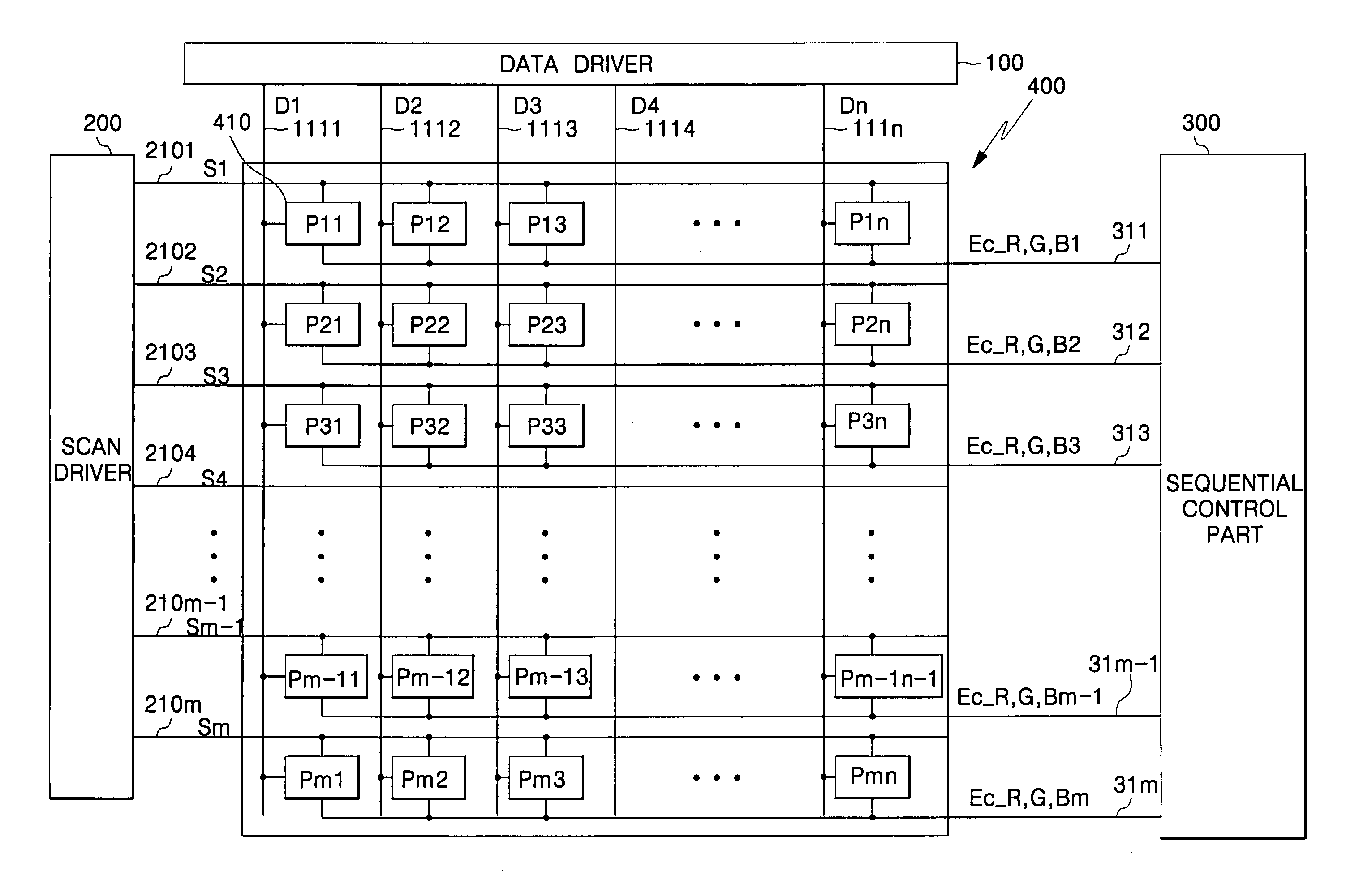
[0073]FIG. 5 is a block diagram of an organic electroluminescent display device according to an exemplary embodiment of the present invention.

[0074] The organic electroluminescent display device illustrated in FIG. 5 includes data driver 100, scan driver 200, sequential control part 300 and pixel part 400. Pixel part 400 includes a plurality of gate lines 2101-210n to which scan signals S1-Sm are supplied from the scan driver 200, a plurality of data lines 1111-111n to which data signals D1-Dm are supplied from the data driver 100, and a plurality of emission control lines 311-31m to which emission control signals EC_R,G,B1-EC_R,G,Bm are supplied from the sequential control part 300.

[0075] The pixel part 400 further includes a plurality of pixels P11-Pmn arranged in a matrix shape and connected to their respective gate lines 2101-210m, data lines 1111-111n, and emission control lines 311-31m.

[0076] According to the illustrated embodiment, pixel P11 is connected to gate line 2101 ...


PUM

PropertyMeasurementUnit
timeaaaaaaaaaa
threshold voltageaaaaaaaaaa
period of timeaaaaaaaaaa

Abstract

A pixel circuit of a display device for improving an opening ratio and a contrast ratio of emitting devices by sharing a driving circuit and sequentially emitting the emitting devices. A data charging period and an emitting period of the emitting devices are divided to prevent flow of wrong data current while data is being stored. The pixel circuit includes red, green, and blue emitting devices and a sequential controller sequentially controlling emission of the emitting devices for a certain sub-frame of a frame. A driving device is coupled to the emitting devices for transmitting driving signals to the emitting devices. A compensation circuit outputs voltage for compensating a threshold voltage of the driving device. The sequential controller controls the emitting devices so that the emitting devices are emitted only for a particular period of time of the subframe.

Description

CROSS-REFERENCE TO RELATED APPLICATION [0001] This application claims priority to and the benefit of Korean Patent Application No. 2003-87794, filed on Nov. 29, 2003, the disclosure of which is hereby incorporated herein by reference in its entirety. BACKGROUND OF THE INVENTION [0002] 1. Field of the Invention [0003] The present invention relates to a driving circuit of an emitting device used in an image display unit, and a method for driving the same. More particularly, the present invention relates to a pixel circuit of a display device for improving an opening ratio and a contrast ratio of the emitting device. [0004] 2. Description of Related Art [0005] A display device, for example, an organic electroluminescent display device is a display device which generates a display by flowing current from a pixel electrode at each pixel to the organic electroluminescent device. The organic electroluminescent display device is generally divided into a passive matrix type organic electrolu...

Claims


Application Information

Patent Timeline
Patent Type & Authority Applications(United States)
IPC IPC(8): G09G3/20G09G3/22G02F1/133G09G3/30G09G3/32G09G3/36H01L51/50
CPCG09G3/2025G09G3/3233G09G3/3283G09G5/02G09G2300/0465G09G2310/0297G09G2300/0814G09G2300/0819G09G2300/0842G09G2310/0235G09G2300/0804G09G3/30
Inventor SHIN, DONG-YONG
Owner SAMSUNG MOBILE DISPLAY CO LTD
Why Eureka
Try Eureka