
Driving circuit for non-volatile DRAM

a non-volatile, random access memory technology, applied in the direction of digital storage, instruments, transistors, etc., can solve the problems of inability to transfer data in parallel from a capacitor to a floating gate in all cells, the method and process of fabricating the dram cell may be more complex, and achieve the effect of easy control of the nvdram

Active Publication Date: 2005-06-30
SK HYNIX INC
View PDF4 Cites 10 Cited by
  • Summary
  • Abstract
  • Description
  • Claims
  • Application Information

AI Technical Summary

Benefits of technology

[0011] It is, therefore, an object of the present invention to provide a non-volatile dynamic random access memory (NVDRAM) having a trapping layer, which can trap electrons or holes, for being easy to control the NVDRAM.

Problems solved by technology

Namely, the ROM can keep stored data even though power supply is removed, but the RAM cannot keep stored data if the power supply is removed.
A main disadvantage of this cell is that data cannot be transferred from a capacitor to a floating gate in parallel in all cells since the DEIS stack is located on the bit line side of the cell.
Also, a method and process for fabricating the DRAM cell may be more complex.
In comparison with a DRAM cell of which a plate line voltage can be adjusted, the NVDRAM may consume larger power because the word line and the bit line should be supplied with a relatively high voltage.
However, in U.S. Ser. No. 10 / 749,356, the NVDRAM should repeatedly carry out a SRC process many times in a normal mode so that charges in a source can not be unlimitedly flowed into a floating gate.
In addition, it is disadvantage that a control for preventing a threshold voltage from increasing because of the charges continuously inputted to the floating gate is more complex.

Method used


Image

  • Driving circuit for non-volatile DRAM
  • Driving circuit for non-volatile DRAM
  • Driving circuit for non-volatile DRAM

Examples


Embodiment Construction

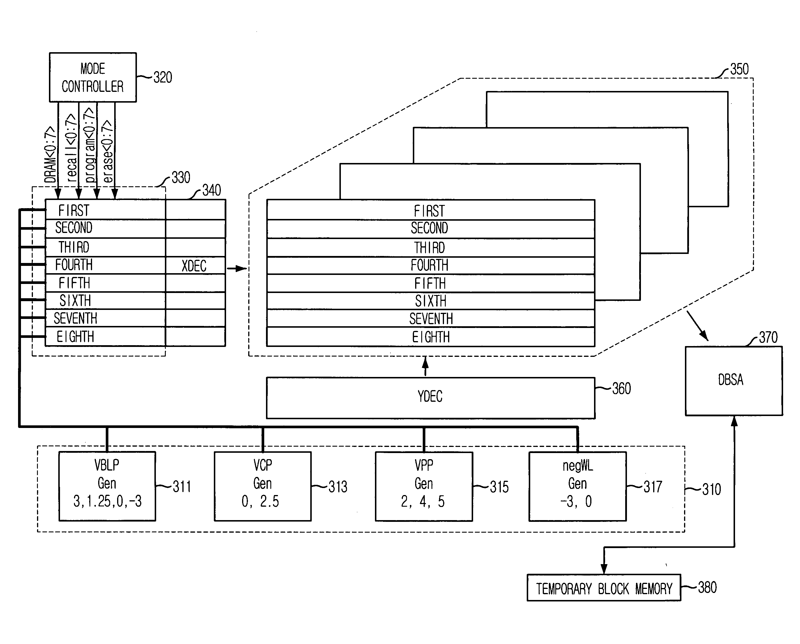
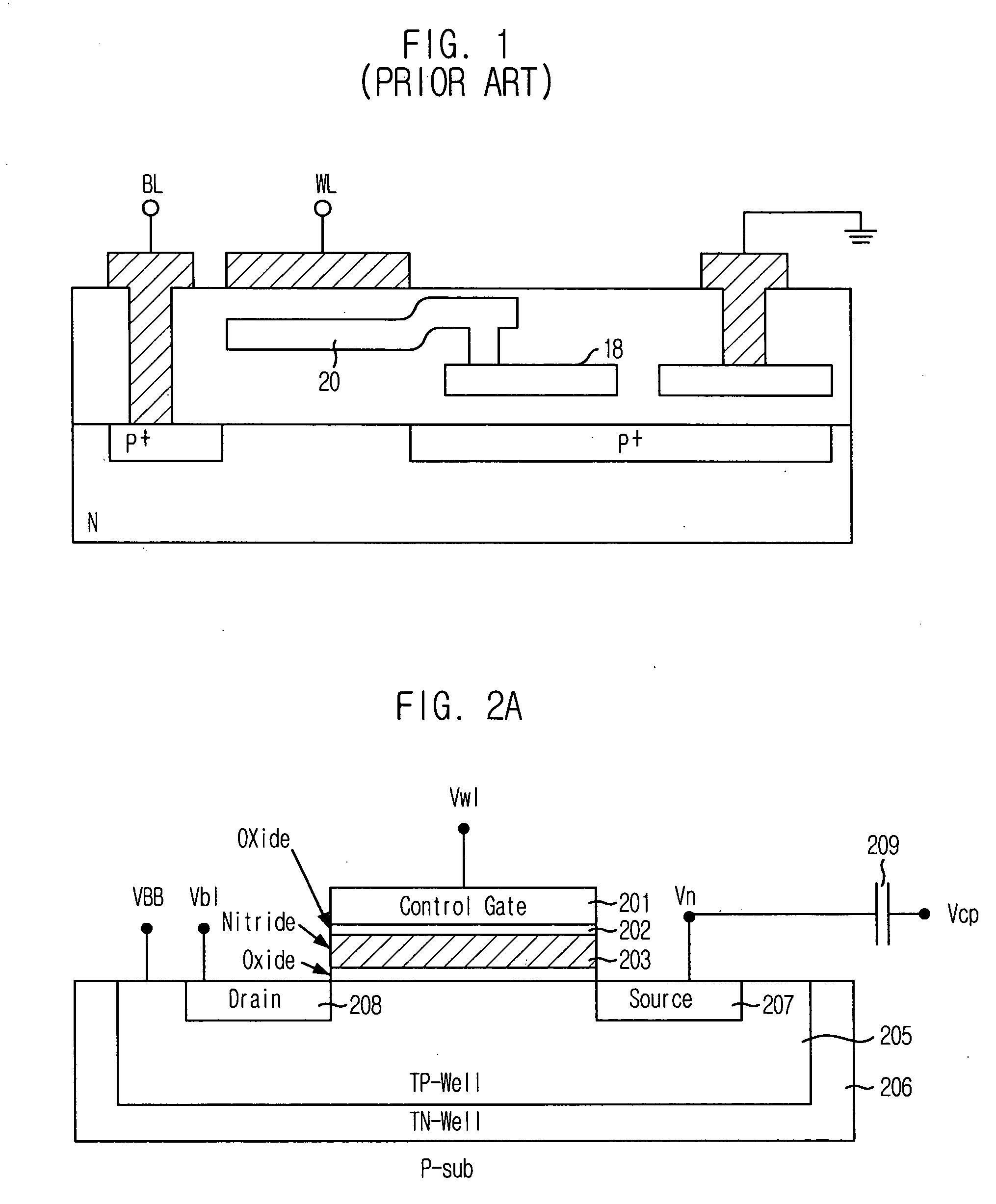
[0023] Hereinafter, a non-volatile dynamic random access memory (NVDRAM) device will be described in detail with reference to the accompanying drawings.

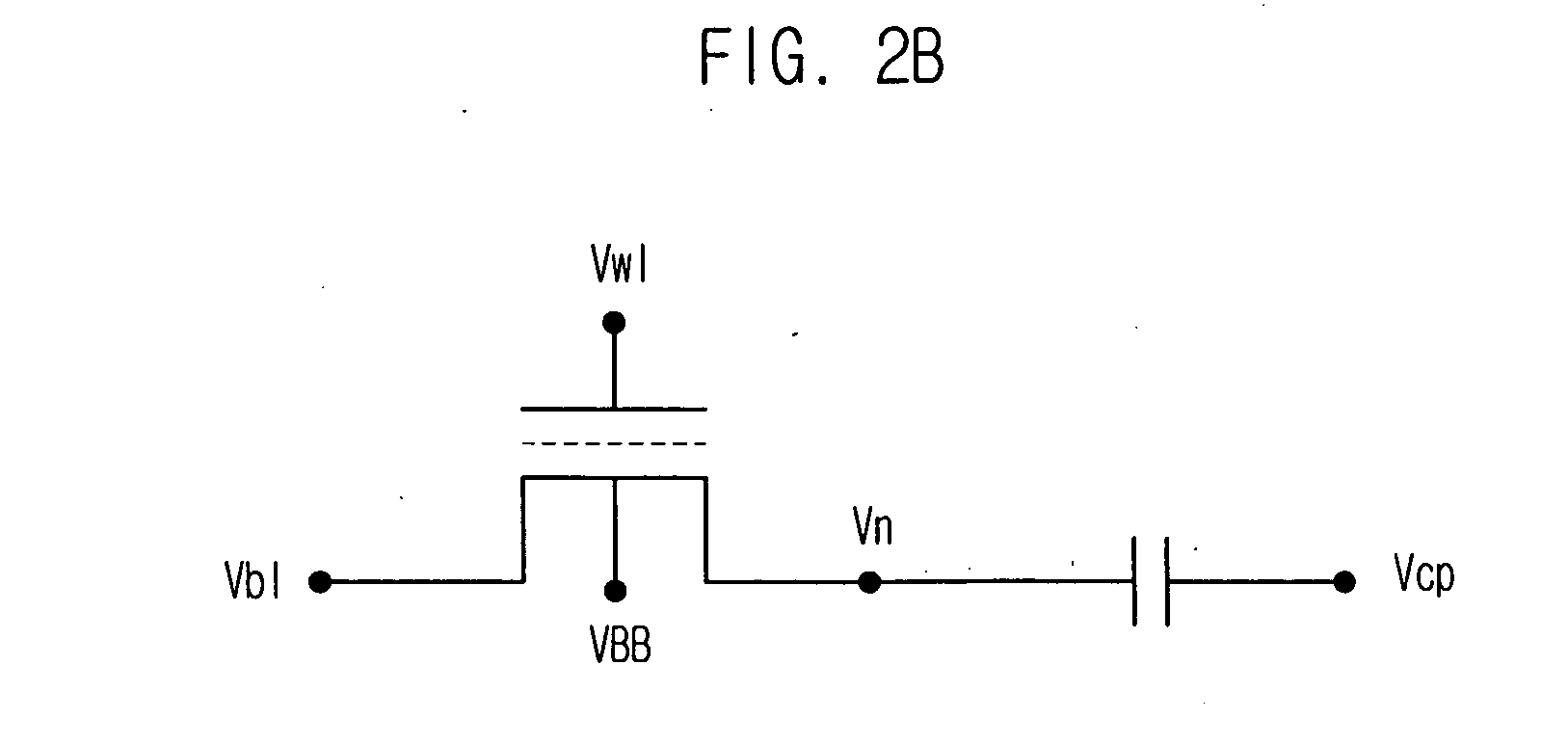
[0024]FIG. 2A is a sectional view showing a unit cell of an NVDRAM in accordance with the present invention. FIG. 2B is a schematic circuit diagram showing a unit cell of the NVDRAM in accordance with the present invention.

[0025] As shown in FIG. 2A, a DRAM cell includes a transistor and a capacitor 209. However, the transistor in the unit cell of the NVDRAM further includes a trapping layer 203 under a control gate 201. Herein, the trapping layer 203 made of non-conductor can trap electrons or holes.

[0026] In the present invention, the trapping layer 203 is provided with a single layer. Also, a plate line of the capacitor 209 is supplied with a plate line voltage Vcp which is controllable, not a fixed voltage, e.g., a ground voltage. As a result, because of the plate line, a size of the unit cell can be decreased. Also, a method ...


PUM


Abstract

A driving circuit for use in a non-volatile dynamic random access memory (NVDRAM) having a nonconductor which can trap electrons or holes includes an internal supply voltage generator for generating the plurality of internal supply voltages, each having at least two different voltage levels; a mode controller for determining an operation mode of the NVDRAM; a voltage level selector for selecting one voltage level of each internal supply voltage in response to the operation mode to thereby outputs the selected voltage level of each internal supply voltage to the row decoding block and the core area; a row decoding block for receiving the internal supply voltages and outputting the internal supply voltages in response to an inputted address; and a core area having a plurality of unit cells, each storing a data, for accessing the data in response to inputted voltage levels of the plurality of internal supply voltages.

Description

FIELD OF INVENTION [0001] The present invention relates to a non-volatile dynamic random access memory (NVDRAM); and, more particularly, to the NVDRAM having a trapping layer which can trap an electron or holes. DESCRIPTION OF PRIOR ART [0002] In general, a semiconductor memory device can be classified into a random access memory (hereinafter, referred as RAM) and a read only memory (hereinafter, referred as ROM). The RAM is volatile, where as the ROM is nonvolatile. Namely, the ROM can keep stored data even though power supply is removed, but the RAM cannot keep stored data if the power supply is removed. [0003] A plurality of RAMs, which take advantage of the ability of field effect transistors to store charge, have evolved and thus serve as memory cells. Such cells may be either dynamic or static in nature. As well know, the dynamic cells may employ only a single field effect transistor and the static cells may be arranged in a flip-flop configuration. These types of the cells ma...

Claims


Application Information

Patent Timeline
Patent Type & Authority Applications(United States)
IPC IPC(8): G11C16/04G11C7/00G11C11/404G11C11/407G11C14/00G11C16/06G11C16/30H01L21/8247H01L27/10H01L29/788H01L29/792H10B69/00
CPCG11C11/404G11C14/00H01L27/115G11C16/30H01L27/105G11C14/0018H10B69/00
Inventor AHN, JIN-HONGHONG, SANG-HOONLEE, SANG-DONKIM, YIL-WOOKPARK, YOUNG-JUNE
Owner SK HYNIX INC
Learn More