Method for forming polycrystalline silicon film

Inactive Publication Date: 2005-06-30
BOE HYDIS TECH
View PDF5 Cites 21 Cited by
  • Summary
  • Abstract
  • Description
  • Claims
  • Application Information

AI Technical Summary

Benefits of technology

[0016] Accordingly, the present invention has been made to solve the above-mentioned problems occurring in the prior art,

Problems solved by technology

However, an a-Si TFT which uses a-Si as the active layer has a very low mobility of about 0.5 cm2/Vs, and thus, has a limitation in making all switching devices included in the liquid crystal display.
In other words, although a driving device for peripheral circuits of the liquid crystal display needs to be operated at very fast speed, the a-Si TFT cannot satisfy an operation speed required in the driving device for peripheral circuits, and thus, it is substantially difficult to realize the drive device for peripheral circuits with the a-Si TFT.
In this method, however, the deformation of the glass substrate occurs at a high temperature above 600° C., thereby causing reductions in reliability and yield.
However, all of the two metho

Method used


Image

  • Method for forming polycrystalline silicon film
  • Method for forming polycrystalline silicon film
  • Method for forming polycrystalline silicon film

Examples


Embodiment Construction

[0026] Hereinafter, a preferred embodiment of the present invention will be described in detail with reference to the accompanying drawings.

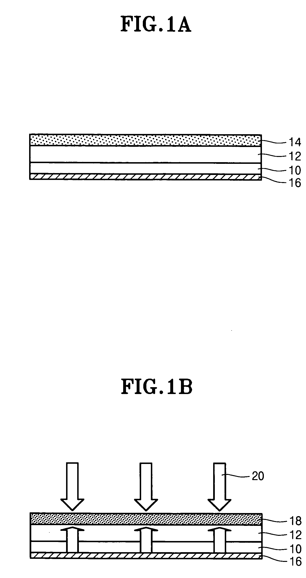
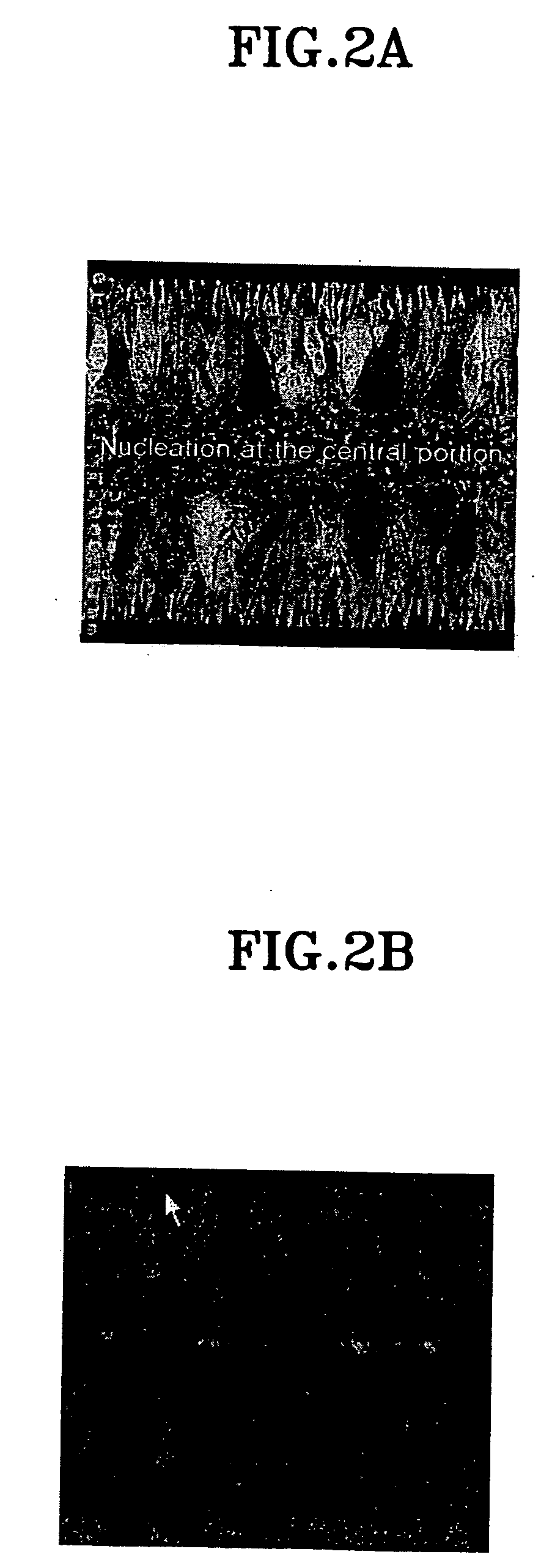
[0027] A technical principle of the present invention will first be described. In conducting a low-temperature crystallization process by excimer laser irradiation, a metal film having high reflectivity is formed on the lower surface of an a-Si film. Thus, in the step of irradiating the a-Si film with laser light, the laser light absorbed into the a-Si film is partially transmitted through the a-Si film, and reflected from the metal film, and then absorbed into the Si film again. Thus, an effect equal to two-step laser irradiation is obtained by one-step laser irradiation, so that the size of grains in a poly-Si film is increased.

[0028] The present invention will now be described in detail with reference to FIGS. 1A and 1B, which are cross-sectional views illustrating a method for forming a poly-Si film according to the present invention. The ...


PUM


Abstract

Disclosed herein is a method for forming a polycrystalline (poly-Si) film by the crystallization of an amorphous silicon film using laser light irradiation. The disclosed method comprises the steps of: sequentially depositing a buffer film and an amorphous silicon film on a glass substrate; depositing a metal film having laser light reflection function on the back side of the glass substrate; and irradiating the front side of the amorphous silicon film with laser light to crystallize the amorphous silicon film. In the laser light irradiation step, the irradiated laser light is absorbed into the amorphous silicon film, and a portion of the absorbed laser light is transmitted through the amorphous silicon film. The transmitted light is reflected from the metal film and absorbed into the amorphous silicon film again, thus crystallizing the amorphous silicon film twice over. According to the present invention, the amorphous silicon film is crystallized twice over so that a polycrystalline film having very large grains can be formed.

Description

BACKGROUND OF THE INVENTION [0001] 1. Field of the Invention [0002] The present invention relates to a method for fabricating a liquid crystal display, and more particularly, to a method for forming a polycrystalline silicon film for polycrystalline silicon thin-film transistors. [0003] 2. Description of the Prior Art [0004] A thin film transistor (hereinafter, referred to as TFT), which is used as a switching device in liquid crystal displays or organic electroluminescent displays, is the most important element in the performance of such displays. Mobility or leakage current, which is a standard for the evaluation of the TFT's performance, greatly depends on the state or structure of an active layer through which an electric charge carrier moves. Namely, this characteristic greatly depends on the state or structure of a silicon thin film which is a material for the active layer. In liquid crystal displays which are currently commercially available, the active layer in TFT is mostly...

Claims


Application Information

Patent Timeline
IPC IPC(8): H01L21/20G02F1/136H01L21/00H01L21/324H01L21/336H01L21/77H01L21/84H01L29/786
CPCH01L21/2026H01L27/1281H01L29/66765H01L29/66757H01L21/02686H01L21/02491H01L21/02488H01L21/02422H01L21/02502H01L21/02678H01L21/02532H01L21/02595H01L21/324H01L21/02675
Inventor SON, KYOUNG SEOKLEE, HO NYEONRYU, MYUNG KWANPARK, JAE CHULKIM, EOK SULEE, JUN HOKWON, SE YEOUL
Owner BOE HYDIS TECH
Why Eureka
Try Eureka