Printable Inorganic Semiconductor Structures

a technology of inorganic semiconductors and semiconductor structures, applied in the direction of solid-state devices, basic electric elements, electric devices, etc., can solve the problems of reducing the performance and acceptability of the resulting led, the high cost of the display, and the resulting led performance reduction, etc., to achieve high-performance

Active Publication Date: 2016-11-17
X DISPLAY CO TECH LTD
View PDF2 Cites 36 Cited by
  • Summary
  • Abstract
  • Description
  • Claims
  • Application Information

AI Technical Summary

Benefits of technology

[0008]The present invention provides structures and methods that enable the construction of micro-devices formed on a sapphire substrate that can be micro-transfer printed. Such printed structures enable low-cost, high-performance arrays of electrically connected micro-devices (e.g., micro-LEDs) useful, for example, in display systems. For example, described herein are micro assembled arrays of micro devices, such as micro-LEDs, that are too small (e.g., micro LEDs with a width, length, height and / or diameter of 0.5 μm to 50 μm; e.g., a width of 1-8 μm, a length of 5-10 μm and a height of 0.5-3 μm), numerous, or fragile to be assembled by conventional means. Rather, these arrays are assembled using micro transfer printing technology. The micro-devices may be prepared on a native substrate and printed to a destination substrate (e.g., plastic, metal, glass, sapphire, transparent materials, or flexible materials), thereby obviating the manufacture of the micro-devices on the destination substrate.
[0011]Moreover, these micro transfer printing techniques may be used to print semiconductor devices at temperatures compatible with assembly on plastic polymer substrates. In addition, semiconductor materials may be printed onto large areas of substrates thereby enabling continuous, high speed printing of complex integrated electrical circuits over large substrate areas.
[0012]Moreover, fully flexible electronic devices with good electronic performance in flexed or deformed device orientations may be provided to enable a wide range of flexible electronic devices. The destination substrate may be flexible, thereby permitting the production of flexible electronic devices. Flexible substrates may be integrated in a large number of configurations, including configurations not possible with brittle silicon based electronic devices. Additionally, plastic substrates, for example, are mechanically rugged and may be used to provide electronic devices that are less susceptible to damage and / or electronic performance degradation caused by mechanical stress. Thus, these materials may be used to fabricate electronic devices by continuous, high speed, printing techniques capable of generating electronic devices over large substrate areas at low cost (e.g., roll to roll manufacturing).
[0014]Vertical LEDs are challenged in electrically isolating the anode and cathode during the process of interconnection. For example, displays that use vertical LED structures require the panel-level formation of vertical electrical insulation between the two terminals of the LEDs. In certain embodiments, the disclosed technology avoids this problem by placing the terminals on the same face of the micro-device, such as a micro-LED. Horizontal separation of contact pads facilitates electrical isolation by dint of the horizontal separation of conductors, thereby bypassing this requirement. Additionally, this allows the connections to the terminals of each micro-device to be formed on a single level, thereby reducing the number of levels in the assembled device and improving placement accuracy.
[0015]In certain embodiments, micro-devices are assembled (e.g., via micro transfer printing) onto the insulator and holes are created in the insulator to access conductive wires below the insulator. A single level of interconnections are used to provide contact to the terminals of the micro-devices. Thus, this architecture reduces the number of levels required to form the display.
[0016]Fine lithography may be used to minimize the separation distance between the terminals (e.g., a separation distance of distance of 100 nm to 20 microns), thus increasing the size of the micro-device terminals. Minimizing the lateral separation between terminals and the micro-device and maximizing the size of the terminals (within the confines of the dimensions of the micro-device) maximizes the tolerance for registration and lithography errors between the assembled micro-devices and the relatively coarse conductive lines used to interconnect them on the display substrate.

Problems solved by technology

However, such displays are expensive to make, in part because of the need for small LEDs and the cost of locating small LEDs on a display substrate.
However, the lattice structure of the sapphire wafer does not match that of the GaN LED crystal and therefore the crystal structure tends to have defects, reducing the performance and acceptability of the resulting LED.
Although relatively inexpensive when compared to sapphire, silicon has an even larger lattice mismatch with the GaN crystal structures making up the LEDs than sapphire, further reducing the performance of the resulting LEDs.
However, there is no available method for undercutting a chiplet formed on a sapphire substrate to enable release of the chiplet for micro-transfer printing.

Method used


Image

  • Printable Inorganic Semiconductor Structures
  • Printable Inorganic Semiconductor Structures
  • Printable Inorganic Semiconductor Structures

Examples


Embodiment Construction

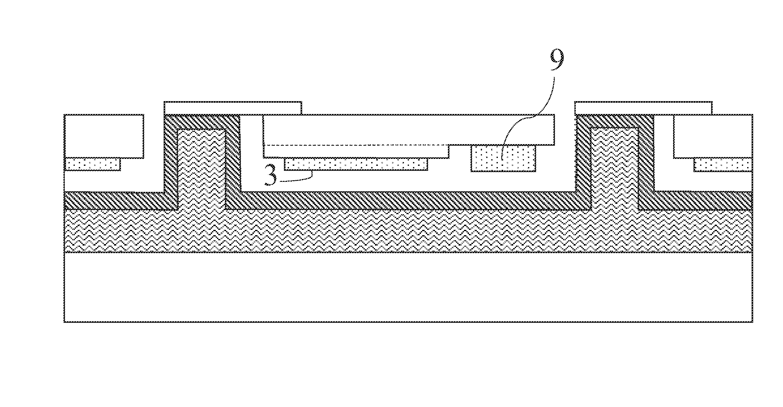
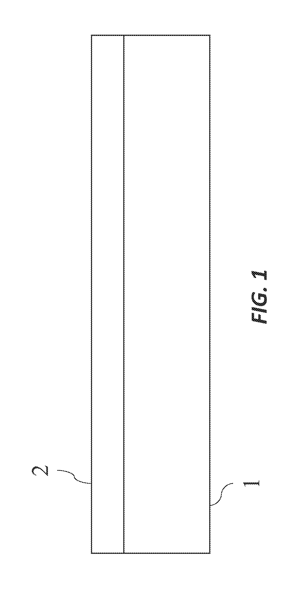
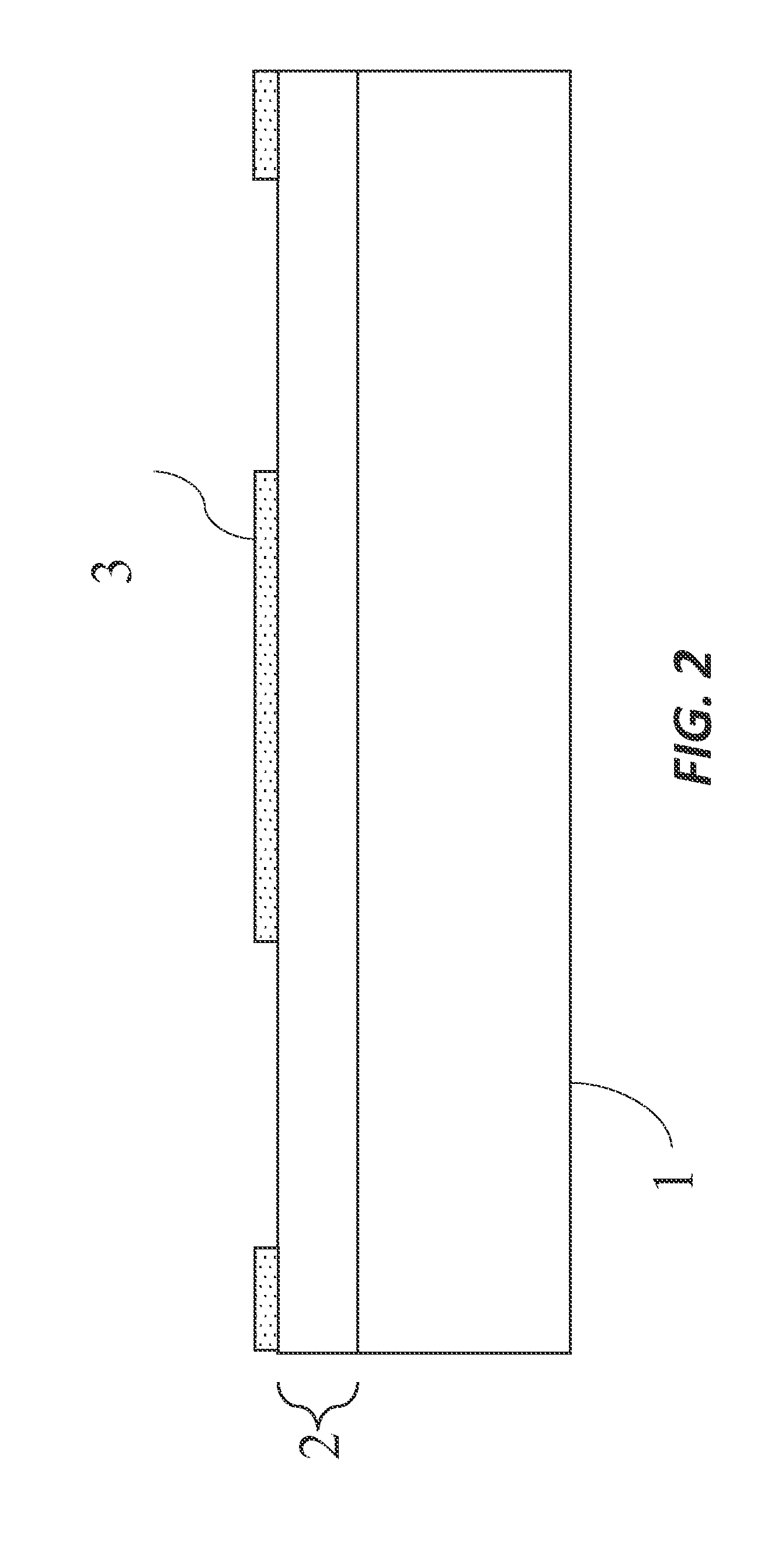
[0088]The present invention provides structures and methods that enable the construction of micro-LED chiplets formed on a substrate that can be micro-transfer printed. Such printed structures enable low-cost, high-performance arrays of electrically connected micro-LEDs useful, for example, in display systems. Furthermore, in an embodiment, the electrical contacts for printed LEDs are electrically interconnected in a single set of process steps. Various semiconductor elements may be formed using the methods and techniques described here, including diode (e.g., micro-diodes), lasers (micro-lasers), light-emitting diode (e.g., micro-LEDs).

[0089]FIGS. 1-10 are diagrams illustrating step-by-step fabrication of a printable semiconductor element 60 secured to an anchor 12 by a tether 10 such that the semiconductor element 60 may be picked up by a transfer device as illustrated in FIG. 16. FIG. 22 is a flowchart illustrating a series of steps (e.g., in sequential order) corresponding to th...


PUM


Abstract

The present invention provides structures and methods that enable the construction of micro-LED chiplets formed on a sapphire substrate that can be micro-transfer printed. Such printed structures enable low-cost, high-performance arrays of electrically connected micro-LEDs useful, for example, in display systems. Furthermore, in an embodiment, the electrical contacts for printed LEDs are electrically interconnected in a single set of process steps. In certain embodiments, formation of the printable micro devices begins while the semiconductor structure remains on a substrate. After partially forming the printable micro devices, a handle substrate is attached to the system opposite the substrate such that the system is secured to the handle substrate. The substrate may then be removed and formation of the semiconductor structures is completed. Upon completion, the printable micro devices may be micro transfer printed to a destination substrate.

Description

FIELD OF THE INVENTION[0001]The present invention relates to structures and methods for providing micro-light-emitting diodes on sapphire substrates that can be printed using massively parallel micro-transfer printing methods.BACKGROUND OF THE INVENTION[0002]Light-emitting diodes (LEDs) are widely used in the display industry as indicators and in small textual or graphic displays. More recently, LEDs are used in large, tiled outdoor displays and have been demonstrated for indoor applications. However, such displays are expensive to make, in part because of the need for small LEDs and the cost of locating small LEDs on a display substrate.[0003]LEDs are formed in a semiconductor material, often using gallium nitride (GaN). These materials are deposited, with suitable doping, on a wafer substrate to form a crystalline structure that is the LED. Electrical contacts are then formed using photolithographic methods and the LED device is singulated from the wafer and packaged. Most LEDs ar...

Claims


Application Information

Patent Timeline
Patent Type & Authority Applications(United States)
IPC IPC(8): H01L33/32H01L33/62H01L33/00
CPCH01L33/32H01L33/007H01L33/0079H01L2933/0025H01L21/6835H01L2933/0016H01L2933/0033H01L33/62H01L33/20H01L2221/68318H01L2221/6835H01L2221/68381H01L2221/68322H01L33/0093H01L2224/24225H01L33/40H01L33/26H01L29/7848H01L33/0095H01L33/38H01L33/36H01L33/44
Inventor BOWER, CHRISTOPHERMEITL, MATTHEWGOMEZ, DAVIDPREVATTE, CARLBONAFEDE, SALVATORE
Owner X DISPLAY CO TECH LTD
Why Eureka
Try Eureka