Organic electronic device and its manufacturing method
a technology of electronic devices and manufacturing methods, applied in thermoelectric devices, non-linear optics, instruments, etc., can solve the problem of a large dependence on the performance of devices
- Summary
- Abstract
- Description
- Claims
- Application Information
AI Technical Summary
Problems solved by technology
Method used
Image

Examples
first embodiment
(First Embodiment)
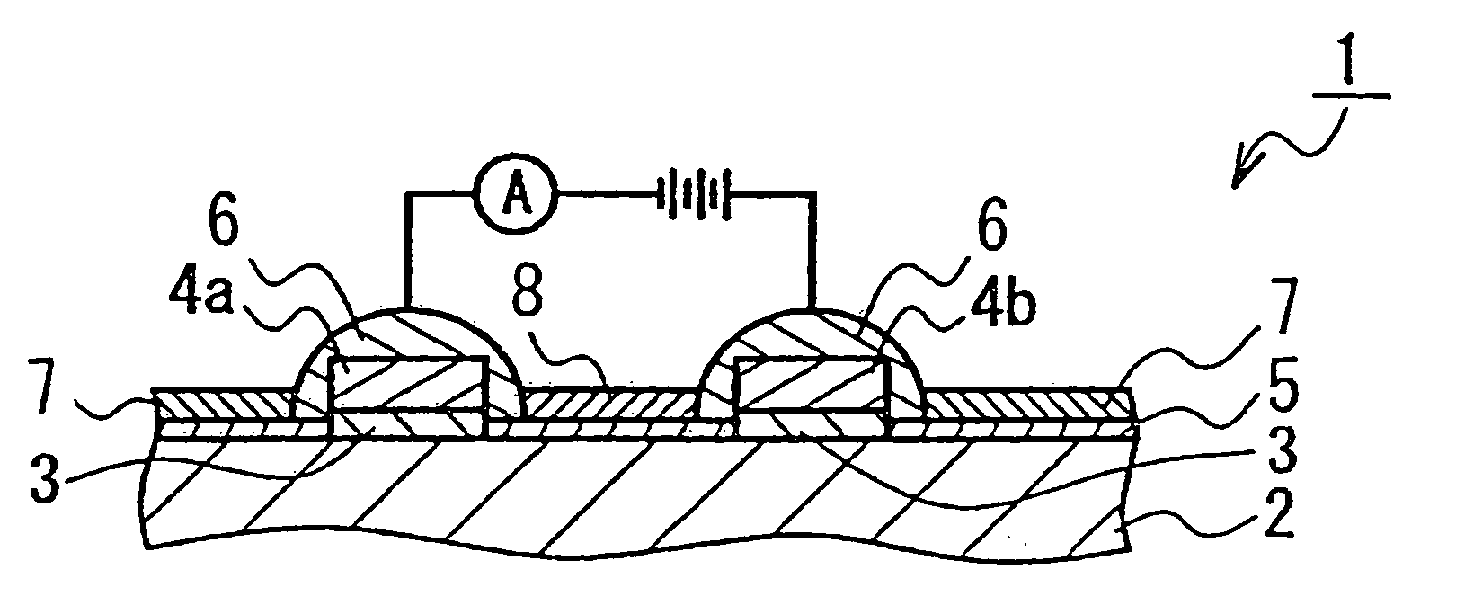
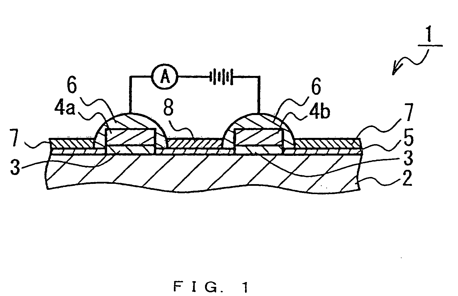
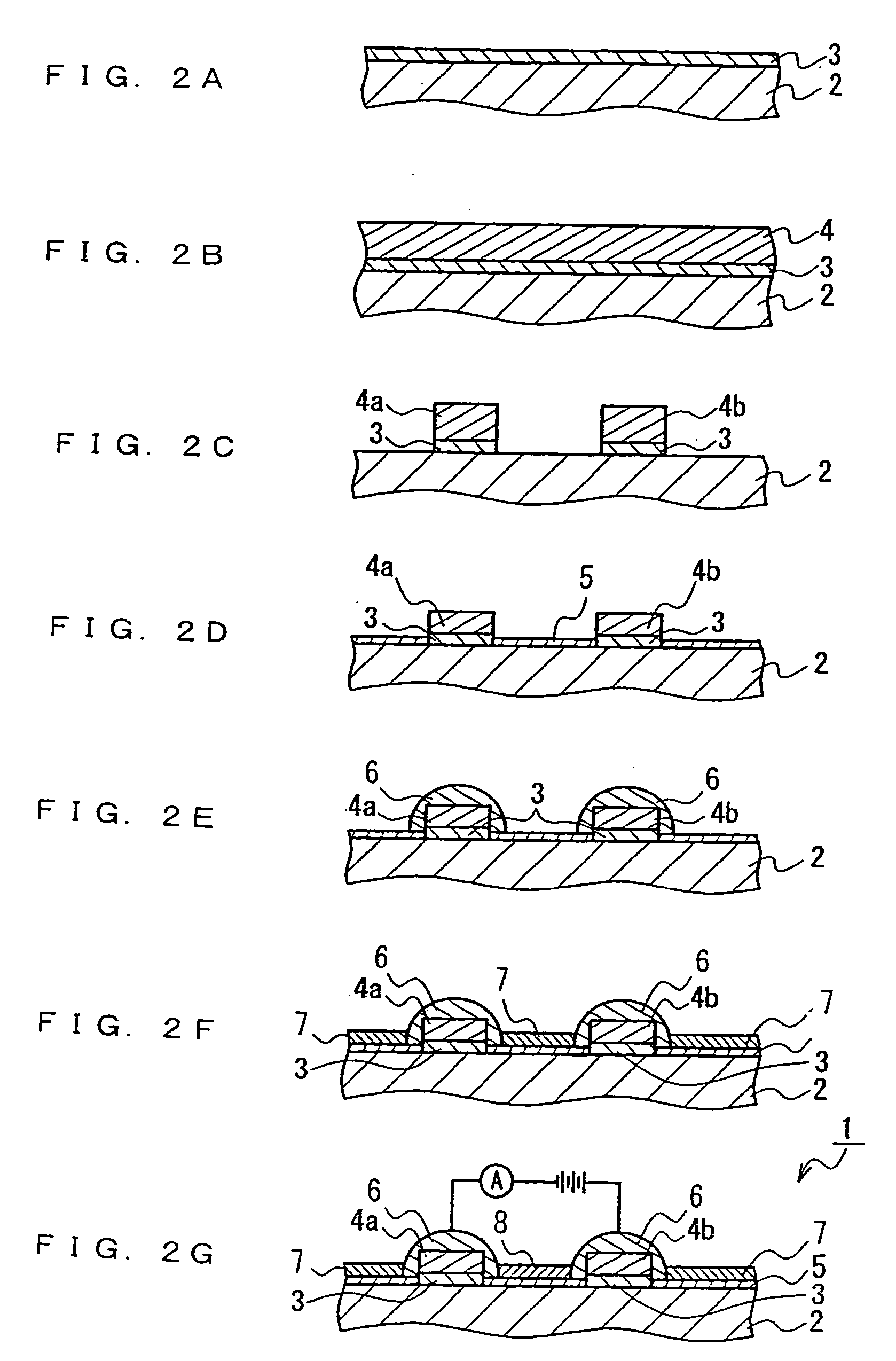
[0116] In this embodiment, a form in which a metal film is used as a coating film will be described. FIG. 1 is a schematic cross-sectional view showing an example of a two-terminal organic electronic device according to this embodiment.
[0117] As shown in FIG. 1, in this organic electronic device 1, an insulating film 3 is formed on a substrate 2, and a first electrode 4a and a second electrode 4b are formed on this insulating film 3 so as to be spaced from each other. Moreover, the first electrode 4a and the second electrode 4b are coated with a metal film for coating 6. Furthermore, on the substrate 2, a conductive organic thin film 8 is formed on the substrate 2 via an insulating film 5 so as to coat a region between the electrodes on the substrate 2. As shown in FIG. 1, the conductive organic thin film 8 is in contact with the electrodes 4a and 4b via the metal film for coating 6. Moreover, on a region of the substrate 2 where the electrodes 4a and 4b and the c...
second embodiment
(Second Embodiment)
[0176] In the above organic electronic device, a layered product containing a plurality of layers of metals or the like also can be used as the electrode. FIG. 6 is a cross-sectional view showing an example of such an organic electronic device, and the same members as in FIG. 1 bear the same numerals.
[0177] This organic electronic device 20 has the same structure as in the first embodiment except that electrodes 4a and 4b are layered products. Examples of the layered product constituting the electrodes 4a and 4b include a layered product containing a layer made of at least one metal selected from the group consisting of Ni, Ti, indium tin oxide (ITO), Cr, and W, and particularly a Ni layer is preferable. There is no particular limitation regarding the number of layers. FIG. 6 illustrates the case where the electrode 4a (4b) is a double-layered product consisting of a lower layer 21a (21b) and an upper layer 22a (22b) as an example, and for such a double-layered p...
third embodiment
(Third Embodiment)
[0181] In this embodiment, a form in which a conductive polymeric film is used as the coating film will be described. FIG. 7 is a cross-sectional view showing an example of such a two-terminal organic electronic device, and the same members as in FIG. 1 bear the same numerals.
[0182] In this organic electronic device 30, an insulating film 3 is formed on a substrate 2 and a first electrode 4a and a second electrode 4b are formed on this insulating film 3 so as to be spaced away from each other as in the first embodiment. In FIG. 7, a form in which the electrodes 4a and 4b are constituted by inner layers 31a and 31b and outer layers 32a and 32b with which the inner layers are coated, respectively, is shown as an example. The electrodes 4a and 4b are coated with polymeric films for coating 33. Furthermore, on the substrate 2, a conductive organic thin film 8 is formed on the substrate 2 via an insulating film 5 so as to coat a region between the electrodes on the sub...
PUM
| Property | Measurement | Unit |
|---|---|---|
| conductivity | aaaaa | aaaaa |
| conductivity | aaaaa | aaaaa |
| conductivity | aaaaa | aaaaa |
Abstract
Description
Claims
Application Information
 - R&D
- Intellectual Property
- Life Sciences
- Materials
- Tech Scout
- Unparalleled Data Quality
- Higher Quality Content
- 60% Fewer Hallucinations
Browse by: Latest US Patents, China's latest patents, Technical Efficacy Thesaurus, Application Domain, Technology Topic, Popular Technical Reports.
© 2025 PatSnap. All rights reserved.Legal|Privacy policy|Modern Slavery Act Transparency Statement|Sitemap|About US| Contact US: help@patsnap.com