Planar package structure for high power light emitting diode

a technology of light-emitting diodes and package structures, which is applied in the direction of basic electric elements, electrical apparatus, and semiconductor devices, can solve the problems of divergent light beams being converged without any particular functions, the volume of the package structure is too large, and the light source of high-power leds with conventional package structures cannot meet the requirements of products with high brightness and compact size, and achieve the effect of reducing the degree of freedom of products and volume of the package structur

Inactive Publication Date: 2005-07-07
IND TECH RES INST
View PDF10 Cites 22 Cited by
  • Summary
  • Abstract
  • Description
  • Claims
  • Application Information

AI Technical Summary

Benefits of technology

[0006] As the LED lamp is utilized with ordinary resin lenses, the volume of package structure is too large and the degree of freedom of the product is reduced.

Problems solved by technology

However, such package structure is too thick and can only make divergent light beams being converged without any particular functions.
Therefore, the light source of high power LED with conventional package structure cannot satisfy the requirements of products with high brightness and compact size in the future.
Another LED package disclosed in U.S. Pat. No. 6,562,643 is also a conventional resin lens-type package, which cannot minimize the thickness of an LED element.
The conventional package structure cannot achieve the requirement of planarization so that variety of the product is greatly limited.
When a point light source is expanded in application to a surface light source, the modulation for achieving light uniformity is difficult.
And, for a large-sized backlight module, too many conventional LEDs are needed such that the production cost of the module is increased.

Method used


Image

  • Planar package structure for high power light emitting diode
  • Planar package structure for high power light emitting diode
  • Planar package structure for high power light emitting diode

Examples


first embodiment

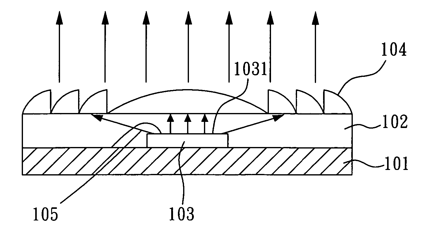
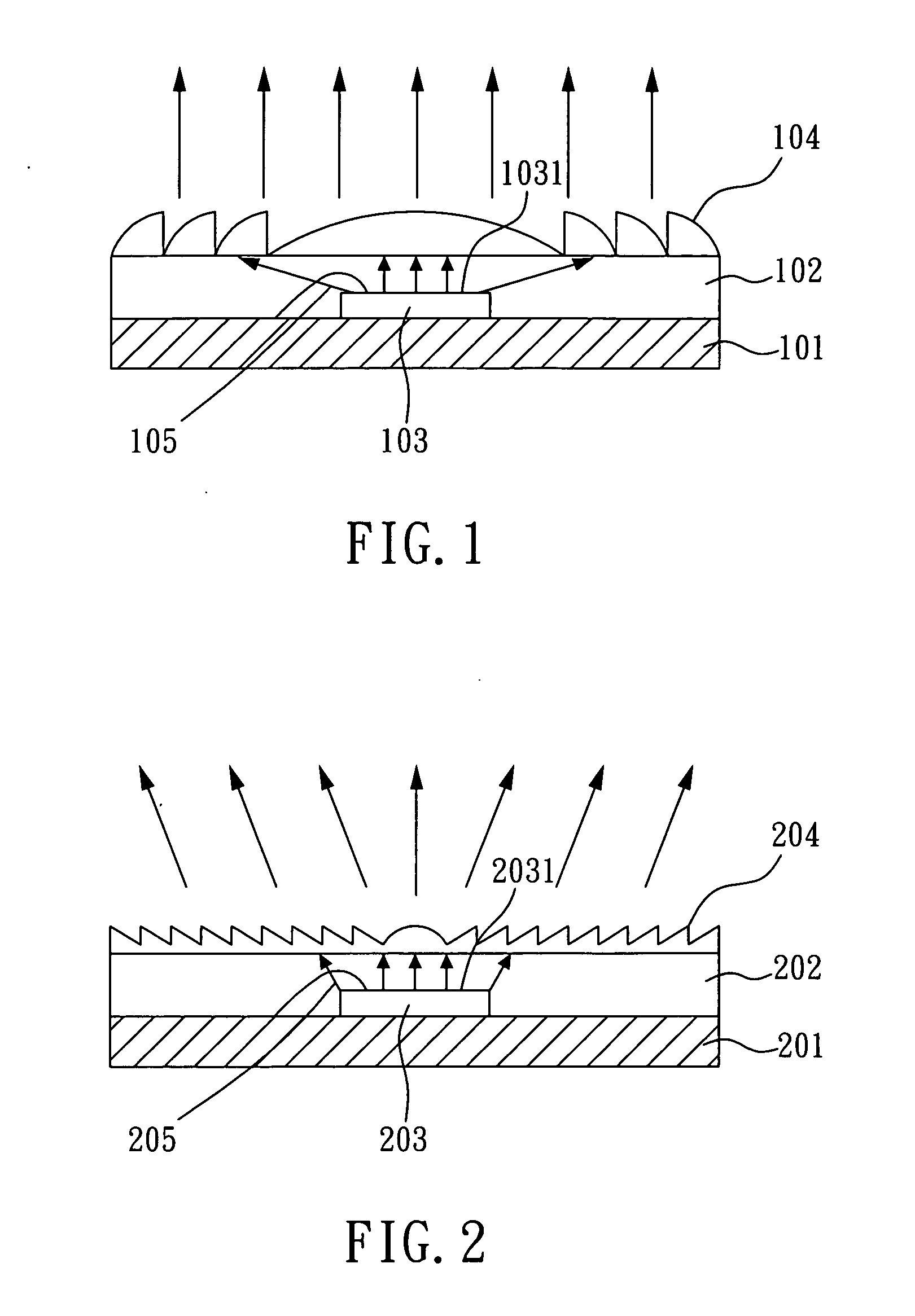
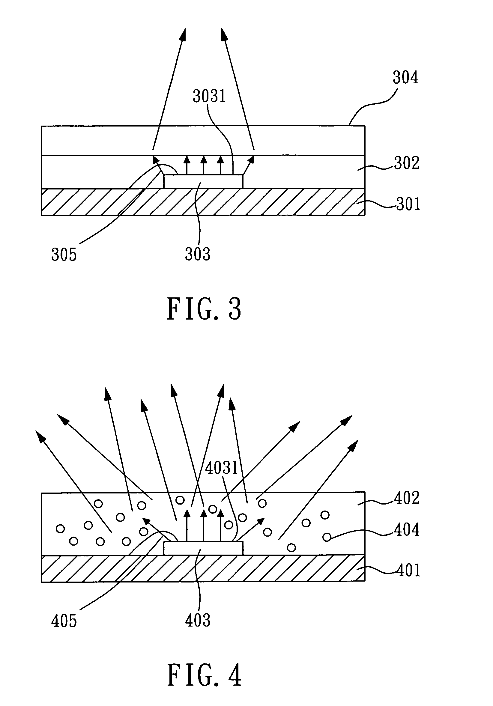
[0024] In the following embodiments of the invention, because most elements are the same as those in the first embodiment, such as substrates 201, 301, 401, 501 are the same as the substrate 101, package materials 202, 302, 402, 502 are the same as the package material 102, LED chips 203, 303, 403, 503a, 503b are the same as the LED chip 103, main light emitting surfaces 2031, 3031, 4031, 5031a, 5031b are the same as the main light emitting surface 1031, descriptions for the structure and function thereof are eliminated thereafter.

[0025] Referring to FIG. 2, which is a cross section of the second embodiment of the invention, the planar optical modulation unit 204 is also a Fresnel lens structure as stated in the first embodiment. However, it performs a diffractive optical phase modulation, i.e. it is formed by a series of concentric rings, wherein the distance between rings and the width of rings can be varied according to the wavelength of the light source 205 to be modulated, the ...

third embodiment

[0026] Referring to FIG. 3, which is a cross section of the invention, the planar optical modulation unit 304 is a lens structure with a gradient refractive index, which is made by doping impurities into a plate-like dielectric to obtain a gradient refractive index. The designed gradient refractive index can refract light beams from the light source 305 to an intended position, i.e. the planar optical modulation unit 304 becomes a lens which has some focal length. Thus, a lens structure with gradient refractive index is formed and the object of flatting the whole package structure is accomplished.

fourth embodiment

[0027] Referring to FIG. 4, which is a cross section of the invention, wherein the package material 402 is doped with a plurality of diffusion particles 404 for scattering light beams from the light source 405, to achieve the effect of diffusing light source. The structure formed by the package material 402 and the diffusion particles 404 is an integrally packaged structure, thus the objects of flatting and integrally packaging are accomplished simultaneously for high power LED.


PUM


Abstract

A planar package structure for high power light emitting diode, comprising: a substrate; a package material; a light emitting diode chip disposed on the substrate, having a main light emitting surface served as a light source; and a planar optical modulation unit disposed on the package material, so that the planar optical modulation unit is above the main light emitting surface, and utilized for modulating the optical phase of the light source. The planar optical modulation unit can perform a refractive optical phase modulation or a diffractive optical phase modulation such that a thin and planar high power light emitting diode package element with function of optical phase modulation is obtained.

Description

1. FIELD OF THE INVENTION [0001] The present invention relates to a planar package structure for high power light emitting diode, and in particular to a thin and planar package structure for high power light emitting diode, which structure is provided with various magnification factors and optical functions by means of the combination of a light emitting diode (LED) chip and a planar lens which has various focal lengths designed by optical calculation and modulation of binary optics and planar lens. 2. BACKGROUND OF THE INVENTION [0002] Conventional package structure for high power LED makes LED lamps have good light emitting directivity such that the light source from the LED chip achieves fine utilization efficiency. However, such package structure is too thick and can only make divergent light beams being converged without any particular functions. Therefore, the light source of high power LED with conventional package structure cannot satisfy the requirements of products with hi...

Claims


Application Information

Patent Timeline
Patent Type & Authority Applications(United States)
IPC IPC(8): H01L33/54H01L33/58
CPCH01L33/58H01L33/54
Inventor YAU, PO-HUNGYANG, JAUH-JUNGLIN, YU-CHENGPAN, I-KAI
Owner IND TECH RES INST
Why Eureka
Try Eureka