Pattern inspection apparatus and method

a technology of pattern inspection and inspection apparatus, which is applied in the direction of image enhancement, instruments, television systems, etc., can solve the problems of fine defects locating in a place except a corner that cannot be detected, and the corner roundness of a pattern formed on a wafer or the like is likely to be detected as a defect, and the pretreatment may not add the corner roundness to the corner roundness

Inactive Publication Date: 2005-07-07
TASMIT INC
View PDF42 Cites 129 Cited by
  • Summary
  • Abstract
  • Description
  • Claims
  • Application Information

AI Technical Summary

Benefits of technology

[0091] According to a twenty-eighth aspect of the present invention, there is provided a pattern inspection apparatus for inspecting a pattern to-be-inspected by using an image of the pattern to-be-inspected and design data for fabricating the pattern to-be-inspected, the pattern inspection apparatus comprising: a reference pattern generation device configured to generate a reference pattern represented by one or more lines from the design data, each of the one or more lines comprising one of a line segment and a curve; an image generation device configured to scan the pattern to-be-inspected with a charged particle beam to generate the image of the pattern to-be-inspected; a detecting device configured to detect an edge of the image of the pattern to-be-inspected; and an inspection device configured to inspect the pattern to-be-inspected by comparing the edge of the image of the pattern to-be-inspected with the one or more lines of the reference pattern; wherein the image generation device scans a given area of the pattern to-be-inspected to generate a hexagonal image thereof, scans an area, adjacent to the given area, of the pattern to-be-inspected to generate a next hexagonal image thereof, and repeatedly scans successive areas of the pattern to-be-inspected to generate a single image of a wide area of the pattern to-be-inspected.
[0092] According to a twenty-ninth aspect of the present invention, there is provided a method of inspecting a pattern to-be-inspected by using an image of the pattern to-be-inspected and design data for fabricating the pattern to-be-inspected, the pattern inspection method comprising: generating a reference pattern represented by one or more lines from the design data, each of the one or more lines comprising one of a line segment and a curve; generating the image of the pattern to-be-inspected; detecting an edge of the image of the pattern to-be-inspected; inspecting the pattern to-be-inspected by comparing the edge of the image of the pattern to-be-inspected with the one or more lines of the reference pattern; and recognizing repeated defects from defect information obtained from the same inspection area with respect to a plurality of semiconductor devices fabricated based on the same design data.
[0093] According to a thirtieth aspect of the present invention, there is provided a method of inspecting a pattern to-be-inspected by using an image of the pattern to-be-inspected and design data for fabricating the pattern to-be-inspected, the pattern inspection method comprising: generating a reference pattern represented by one or more lines from the design data, each of the one or more lines comprising one of a line segment and a curve; generating the image of the pattern to-be-inspected; detecting an edge of the image of the pattern to-be-inspected; and inspecting the pattern to-be-inspected by comparing the edge of the image of the pattern to-be-inspected with the one or more lines of the reference pattern; wherein the reference pattern suitable for inspection using a plurality of the edges is extracted by using at least one of geometrical informatio...

Problems solved by technology

However, by using the die-to-database comparison method for wafer inspection, corner roundness of a pattern formed on a wafer or the like is likely to be detected as a defect.
However, corner roundness added by the pretreatment may be different from corner roundness of each pattern actually formed on the wafer.
As a result, a problem in which a fine defect locating in a place except a corner cannot be detected has happened.
However, the above problem is severe for the die-to-database comparison wafer inspection, because a pattern formed on the wafer is allowed to be deformed as long as an electrical characteristic is guaranteed.
Therefore, the die-to-database comparison wafer inspection has not been put into practical use.
Because the repeated defects occur in the die to-be-inspected and in the adjacent dies that are to be compared with the die to-be-inspected, the die-to-die comparison wafer inspection cannot detect the repeated defects.
Although it has not been put into practical use because of calculation cost or the like, there has been proposed an inspection method using the design data and the wafer image.
However, these methods fail to realize an inspection speed that is usable in high-speed inspection, and fail to perform the matching while detecting a pattern deformation quantity.
However, the method cannot classify whether a killer defect or not, because it is not recognized which part of a circuit is destroyed by the defect.
Moreover, position of a defect detected by the die-to-die comparison inspection has an error caused by precision of a stage and an optical system of an inspection apparatus, and such error is approximately ten or more times larger than a wiring pattern.
Due to the error, even if a defect position is related with the design data, relationship between the defect position and the design data cannot be recognized.
If the OPC pattern does not effectively correct a pattern formed on a wafer, repeated defect occurs.
However, the die-to-die comparison wafer inspection cannot detect the repeated defect.
In addition, in a multi-product/small-volume fabricat...

Method used


Image

  • Pattern inspection apparatus and method
  • Pattern inspection apparatus and method
  • Pattern inspection apparatus and method

Examples


Embodiment Construction

[0251] Contents

[0252] 1. Overview

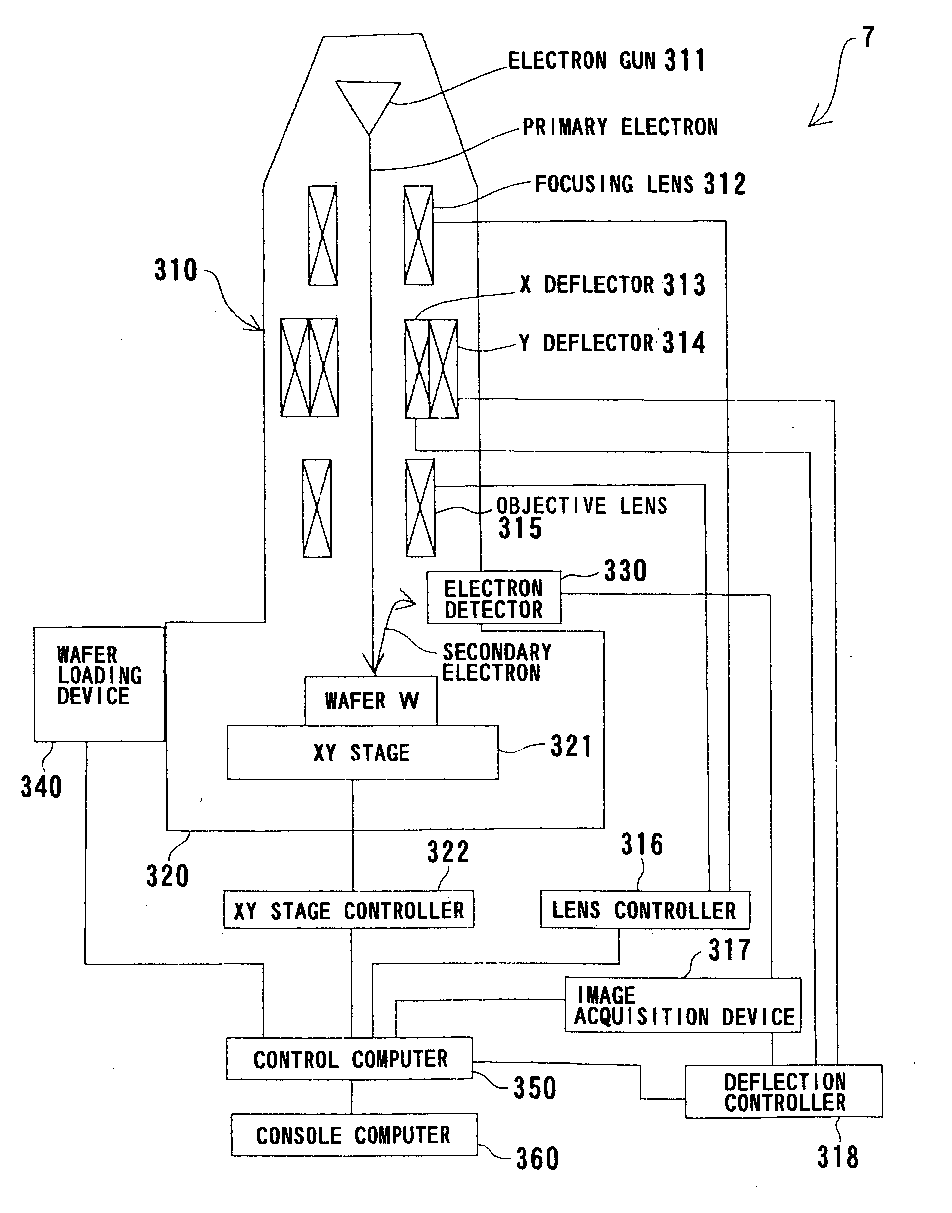
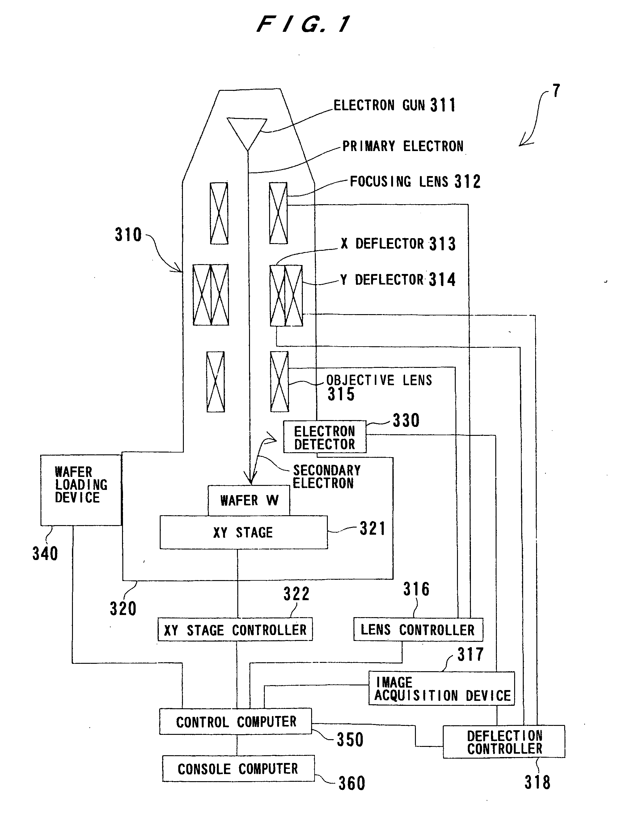
[0253] 2. Hardware configuration

[0254] 2.1 Basic arrangement of image generation device

[0255] 2.2 Scan methods of image generation device

[0256] 2.2.1 Scan method 1

[0257] 2.2.2 Scan method 2

[0258] 2.2.3 Scan method 3

[0259] 2.3 Basic arrangement of pattern inspection apparatus

[0260] 2.4 Functional block diagram

[0261] 3. Explanations of terms
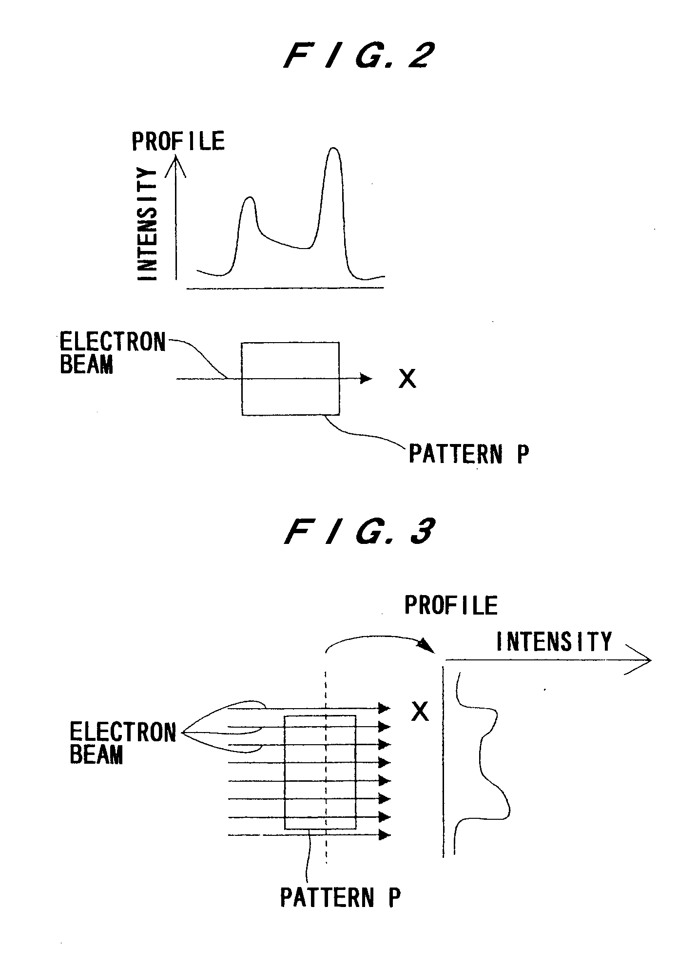
[0262] 3.1 Edge

[0263] 3.2 Reference pattern

[0264] 3.3 Recipe data

[0265] 3.4 Inspection-unit-area

[0266] 3.5 Inspection result

[0267] 4. Basic Inspection processing

[0268] 4.1 The first edge detection

[0269] 4.1.1 The first edge detection method 1

[0270] 4.1.2 The first edge detection method 2

[0271] 4.2 Line-shaped pattern matching method

[0272] 4.2.1 Matching method using unique pattern

[0273] 4.2.2 Matching method using negative pattern

[0274] 4.2.3 Matching method using projection data obtained by projecting edge on the horizontal and vertical axes

[0275] 4.3 Matching method using geometrical inform...


PUM


Abstract

A pattern inspection apparatus is used for inspecting a pattern, such as semiconductor integrated circuit (LSI), liquid crystal panel, and a photomask by using an image of the pattern to-be-inspected and design data for fabricating the pattern to-be-inspected. The pattern inspection apparatus includes a reference pattern generation device for generating a reference pattern represented by one or more lines from design data, an image generation device for generating the image of the pattern to-be-inspected, a detecting device for detecting an edge of the image of the pattern to-be-inspected, and an inspection device for inspecting the pattern to-be-inspected by comparing the edge of the image of the pattern to-be-inspected with the one or more lines of the reference pattern.

Description

[0001] This is a continuation-in-part application of U.S. application Ser. No. 10 / 689,021 filed Oct. 21, 2003, which is a continuation-in-part application of U.S. application Ser. No. 09 / 648,372 filed Aug. 25, 2000.BACKGROUND OF THE INVENTION [0002] 1. Field of the Invention [0003] The present invention relates to a pattern inspection apparatus and a method, and more particularly to a pattern inspection apparatus and a method of inspecting a fine pattern, such as a semiconductor integrated circuit (LSI), a liquid crystal panel, and a photomask (reticle) for the semiconductor or the liquid crystal panel, which are fabricated based on design data. [0004] 2. Description of the Related Art [0005] For the pattern inspection of a wafer in fabricating process of semiconductor integrated circuit or the pattern inspection of a photomask for pattern formation thereof, an optical pattern inspection apparatus that uses the die-to-die comparison method has been used. In the die-to-die comparison...

Claims


Application Information

Patent Timeline
IPC IPC(8): G01B11/00G01N21/00G06T7/00
CPCG06K9/00G06T2207/30148G06T7/0004G06K2209/19G06V2201/06G06F18/00
Inventor KITAMURA, TADASHIKUBOTA, KAZUFUMINAKAZAWA, SHINICHIVOHRA, NEETIYAMAMOTO
Owner TASMIT INC
Why Eureka
Try Eureka