CMOS image sensor and method for fabricating the same

a technology of image sensor and cmos, which is applied in the direction of electrical equipment, semiconductor devices, radio frequency controlled devices, etc., can solve the problems of high power consumption of ccd, inability to realize signal processing circuits within ccd chips, and complicated driving modes

Active Publication Date: 2005-07-21
DONGBU HITEK CO LTD
View PDF3 Cites 41 Cited by
  • Summary
  • Abstract
  • Description
  • Claims
  • Application Information

AI Technical Summary

Benefits of technology

[0030] In forming the device isolation film surrounding the photodiode, since a heavily doped impurity ion region of P type conductivity opposite to the n− region of the photodiode is previously fo

Problems solved by technology

That is, the CCD requires much power consumption and its driving mode is complicated.
Also, since a lot of mask process steps are required, a signal processing circuit cannot be realized within a CCD chip.
At this time, a defect occurs in a corresponding substrate due to ions implanted into the boundary between the device isolation film and the active region.
This defect due to ion implantation causes charge or hole carrier and

Method used


Image

  • CMOS image sensor and method for fabricating the same
  • CMOS image sensor and method for fabricating the same
  • CMOS image sensor and method for fabricating the same

Examples


Embodiment Construction

[0039] Reference will now be made in detail to the preferred embodiments of the present invention, examples of which are illustrated in the accompanying drawings. Wherever possible, the same reference numbers will be used throughout the drawings to refer to the same or like parts.

[0040] Hereinafter, a CMOS image sensor according to the present invention and a method for fabricating the same will be described as follows.

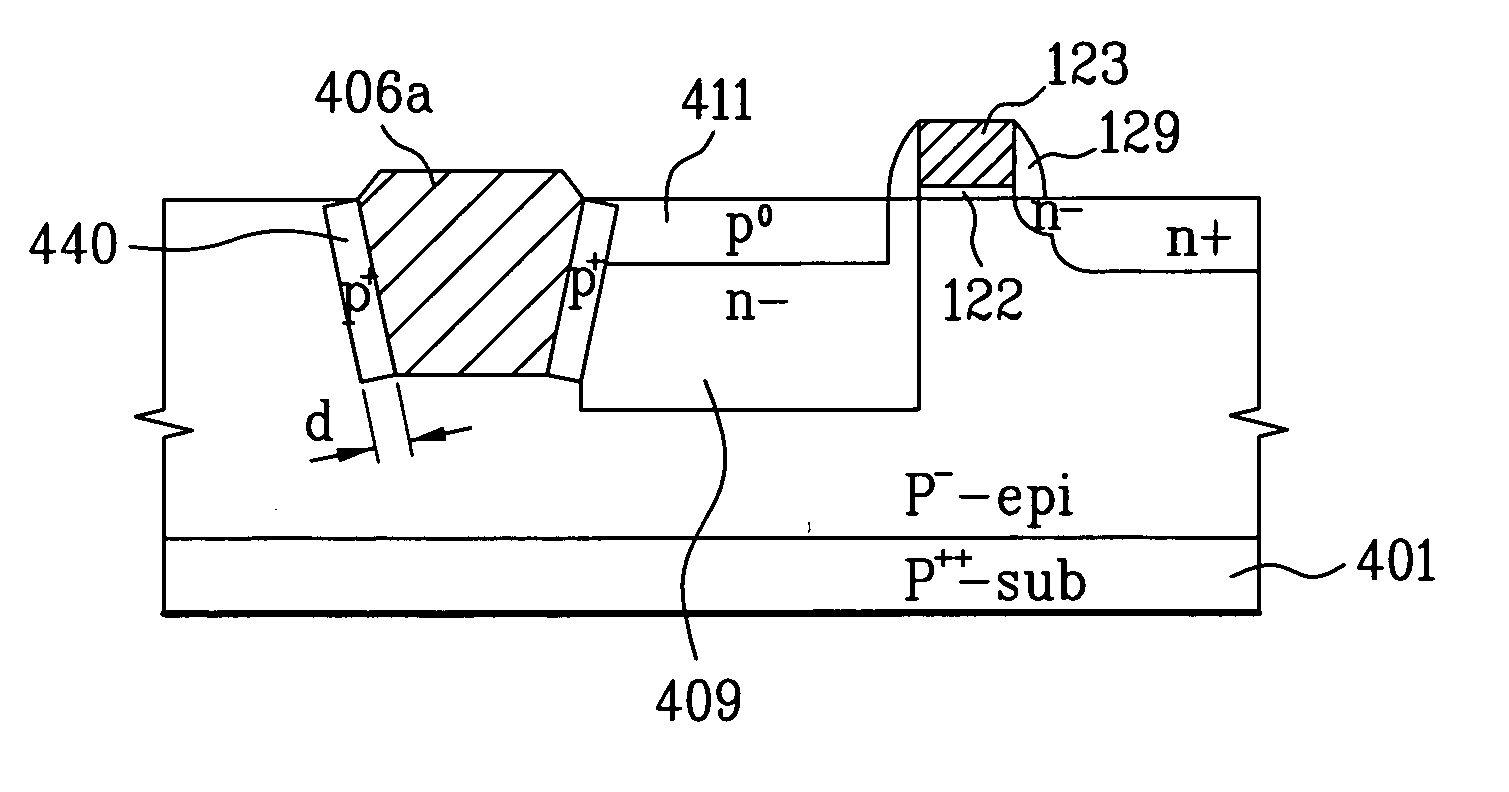
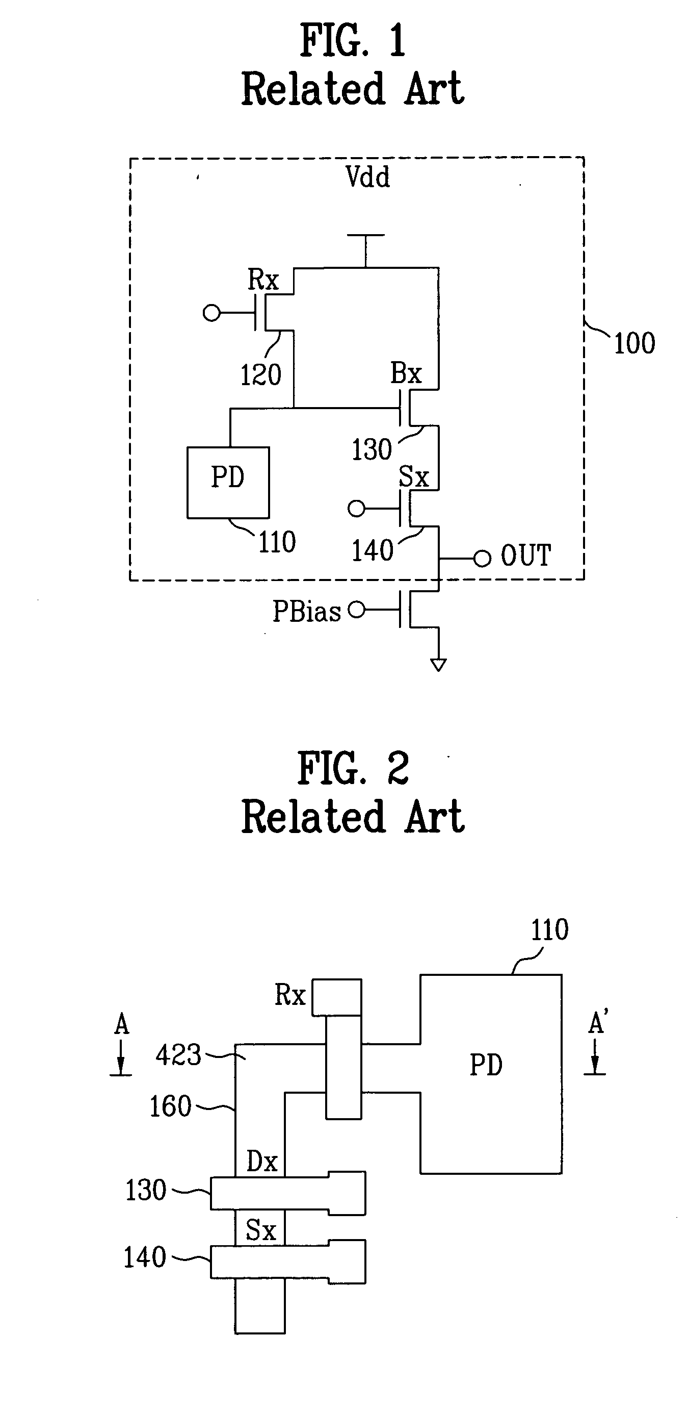
[0041]FIG. 6 is a layout illustrating a unit pixel of a CMOS image sensor according to the present invention. As shown in FIG. 6, an active region is defined by a field region. The active region corresponds to a region inside a solid line 423 in FIG. 6. A gate electrode of a reset transistor Rx 120, a gate electrode of a driver transistor Dx 130, and a gate electrode of a select transistor Sx 140 are arranged to overlap a predetermined portion of the active region. A photodiode PD is formed at one side of the active region. An impurity ion region of the same conduct...


PUM


Abstract

A CMOS image sensor and a method for fabricating the same are disclosed, in which the boundary between an active region and a field region is not damaged by ion implantation. The method for fabricating a CMOS image sensor includes forming a trench in a first conductive type semiconductor substrate, forming a first conductive type heavily doped impurity ion region in the semiconductor substrate at both sides of the trench, forming a device isolation film by interposing an insulating film between the trench and the device isolation, sequentially forming a gate insulating film and a gate electrode on the semiconductor substrate, and forming a second conductive type impurity ion region for a photodiode in the semiconductor substrate between the gate electrode and the device isolation film.

Description

[0001] This application claims the benefit of the Korean Application No. P2003-101553 filed on Dec. 31, 2003, which is hereby incorporated by reference. BACKGROUND OF THE INVENTION [0002] 1. Field of the Invention [0003] The present invention relates to a CMOS image sensor and a method for fabricating the same, and more particularly, to a CMOS image sensor and a method for fabricating the same in which the boundary between an active region and a field region is not damaged by ion implantation. [0004] 2. Discussion of the Related Art [0005] Generally, an image sensor means a semiconductor device converting optical images into electrical signals. The image sensor is divided into a charge coupled device (CCD) and a complementary MOS (CMOS) image sensor. The CCD transfers and stores charge carrier to and in a capacitor in a state that respective MOS capacitors lie adjacent to each other. The CMOS image sensor employs a switching mode that provides MOS transistors by the number of pixels...

Claims


Application Information

Patent Timeline
IPC IPC(8): H01L21/265H01L21/76H01L21/8238H01L27/146H01L31/062H01L31/10
CPCH01L27/14609H01L27/14689H01L27/1463H01L27/146H01L31/10
Inventor HAN, CHANG HUNKIM, BUM SIK
Owner DONGBU HITEK CO LTD
Why Eureka
Try Eureka