Semiconductor device with raised segment

a technology of semiconductors and segments, applied in the field of semiconductor devices, can solve the problems of increasing the difficulty of body-doping concentration, gate oxide thickness, and the inability to meet the requirements of source/drain doping profiles to control short-channel effects, and achieving the effect of small thickness, easy formation of raised source and drain structures

Active Publication Date: 2005-07-21
TAIWAN SEMICON MFG CO LTD
View PDF15 Cites 12 Cited by
  • Summary
  • Abstract
  • Description
  • Claims
  • Application Information

AI Technical Summary

Benefits of technology

[0014] An advantage of a preferred embodiment of the present invention is providing an inexpensive method of forming raised structures over a semiconductor material, which is particularly advantageous in a MOSFET device formed on an SOI wafer or in a UTB application. Advantageously, a deposition or epitaxial growth step is not required; the raised structures are formed by heating the wafer.
[0015] Another advantage of embodiments of the present invention is that a wide process window is provided for forming a raised source and drain structure. In particular, embodiments of the invention allow a raised source and drain structure to be formed with ease, even when the thickness of the silicon body is extremely thin, e.g. less than 100 Angstroms. For example, in prior art methods of forming a raised source and drain structure using epitaxial techniques, it is extremely difficult to grow a semiconductor material selectively on a semiconductor region with a very small thickness.

Problems solved by technology

As the gate length of MOSFET devices is scaled down into the sub-100 nm regime for improved performance and density, the requirements for body-doping concentration, gate oxide thickness, and source / drain doping profiles to control short-channel effects become increasingly difficult to meet when conventional semiconductor device structures based on bulk silicon (Si) substrates are utilized.
Heavy channel 114 doping is required to provide adequate suppression of short-channel effects, which results in degraded mobility and enhanced junction leakage.
The aggressive reduction of the SiO2 gate dielectric 108 thickness for reduced short-channel effects and improved drive current leads to increased direct tunneling gate leakage current and standby power consumption, and also raises concerns regarding the gate dielectric 108 reliability.
However, if ultra-thin source / drain regions 204 and 206 are used for the UTB MOSFET device 200, a high series resistance results that degrades the drive current.
However, selective epitaxial growth of the raised source and drain regions 222 is costly, and the epitaxial growth is highly dependent on the pattern density.

Method used


Image

  • Semiconductor device with raised segment
  • Semiconductor device with raised segment
  • Semiconductor device with raised segment

Examples


Embodiment Construction

[0027] The making and using of the presently preferred embodiments are discussed in detail below. It should be appreciated, however, that the present invention provides many applicable inventive concepts that can be embodied in a wide variety of specific contexts. The specific embodiments discussed are merely illustrative of specific ways to make and use the invention, and do not limit the scope of the invention.

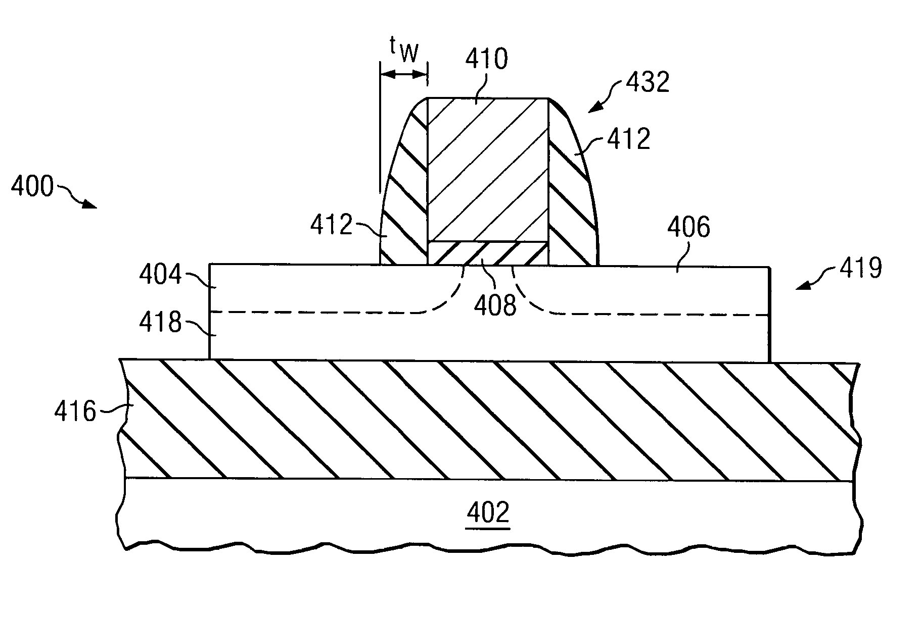
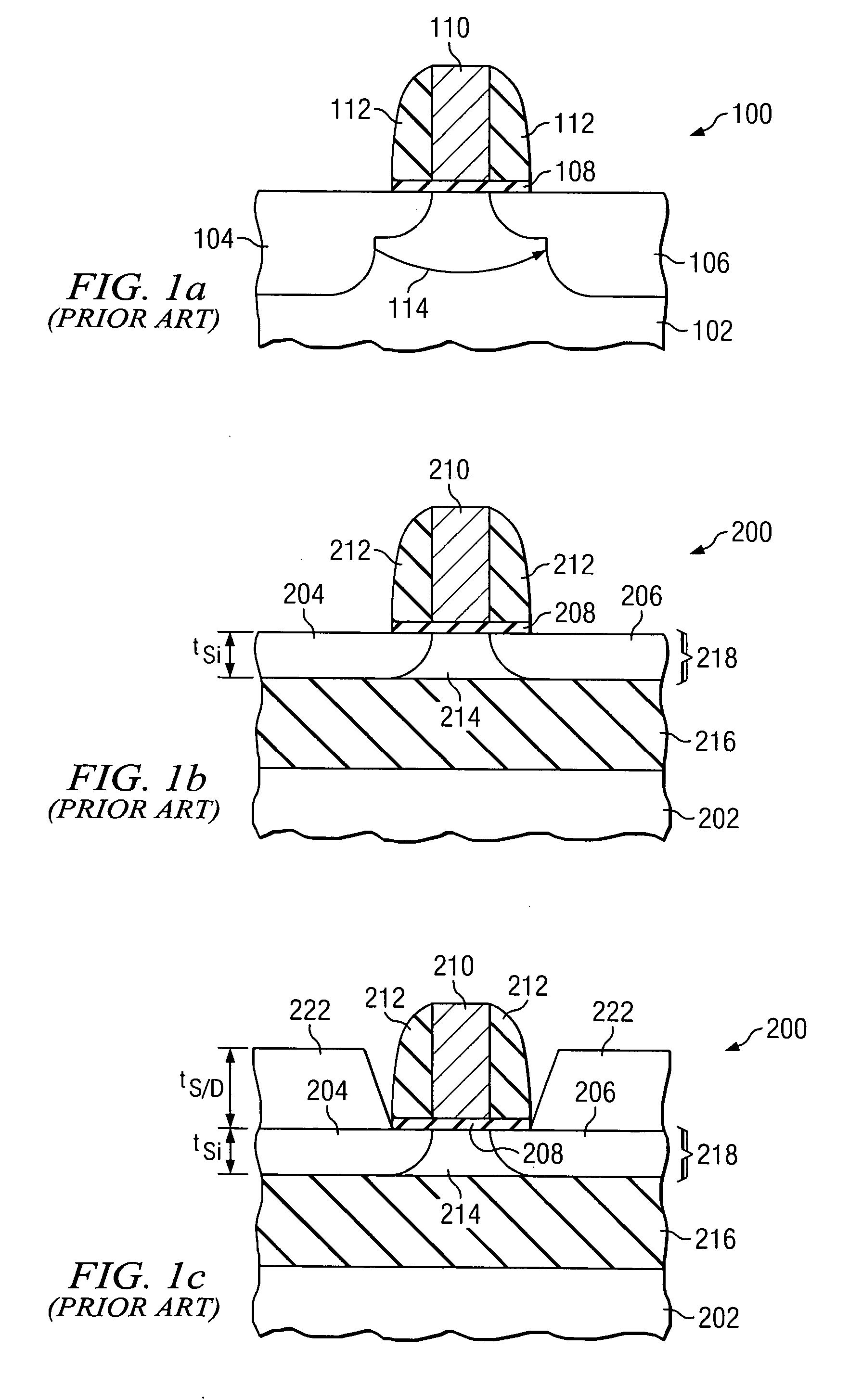
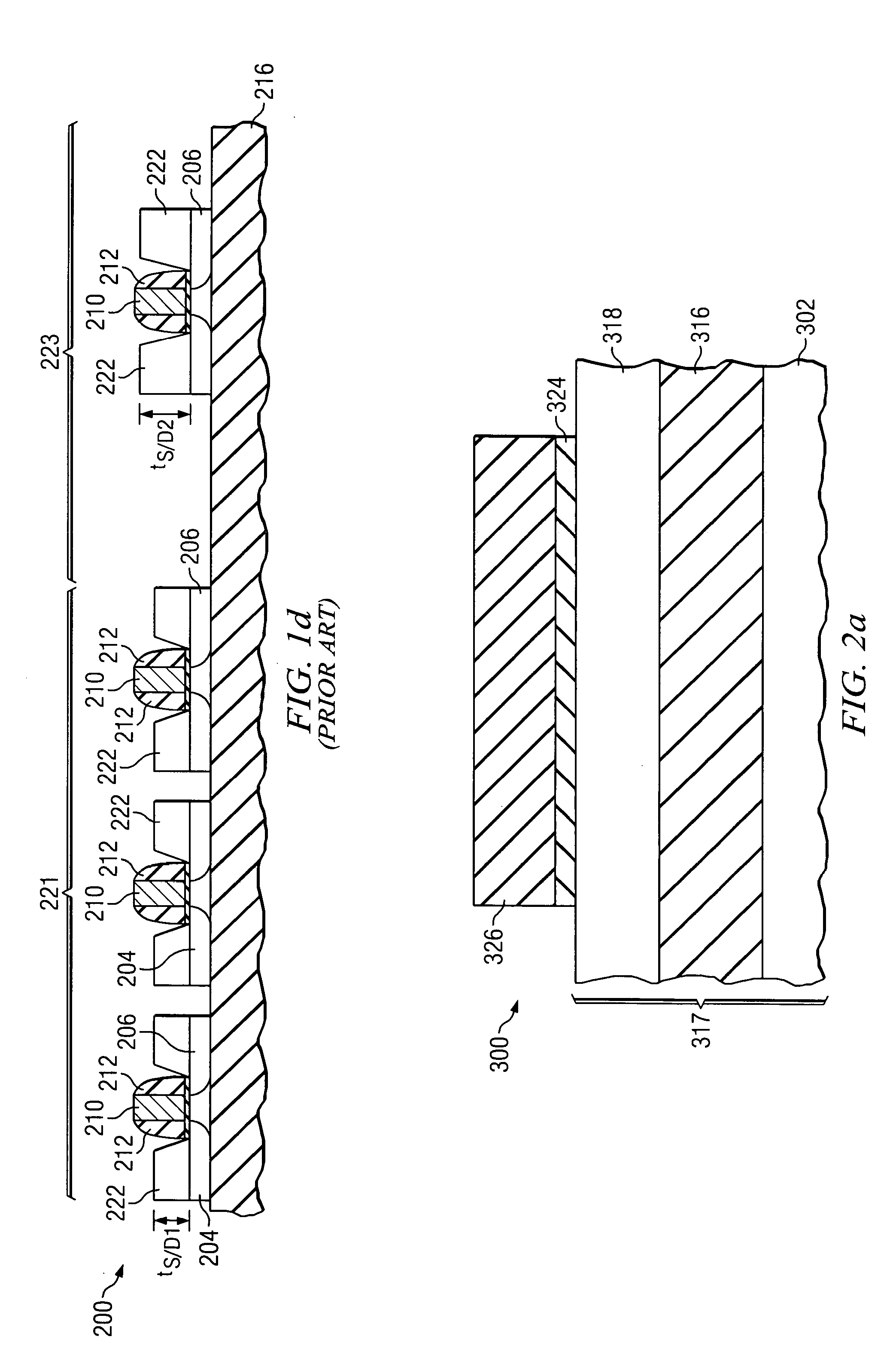
[0028] Embodiments of the present invention will be described herein with respect to preferred embodiments in a specific context, namely a MOSFET device formed within an SOI wafer. Embodiments of the invention may also be applied, however, to other transistors and semiconductor devices, as examples. The method described herein is not restricted to the formation of a raised source and drain region of a semiconductor device; the method may alternatively be used to form a raised segment of any semiconductor device, wherein the raised segment may be a part of a semiconductor de...


PUM


Abstract

A device having a raised segment, and a manufacturing method for same. An SOI wafer is provided having a substrate, an insulating layer disposed over the substrate, and a layer of semiconductor material disposed over the insulating layer. The semiconductor material is patterned to form a mesa structure. The wafer is annealed to form a raised segment on the mesa structure.

Description

TECHNICAL FIELD [0001] The present invention relates generally to the field of semiconductor devices, and more specifically to the fabrication of field effect transistors with raised or elevated source and drain structures. BACKGROUND [0002] Integrated circuits comprising semiconductor devices are used in many electronic applications, such as computers, televisions, cellular phones and other electronic devices. Integrated circuits are continually being designed in smaller dimensions, based on the demand for smaller consumer products and increased speed. Improved yields may also be achieved by reducing the area of an integrated circuit die. [0003] A common component of an integrated circuit is a metal oxide semiconductor field effect transistor (MOSFET). As the gate length of MOSFET devices is scaled down into the sub-100 nm regime for improved performance and density, the requirements for body-doping concentration, gate oxide thickness, and source / drain doping profiles to control sh...

Claims


Application Information

Patent Timeline
Patent Type & Authority Applications(United States)
IPC IPC(8): H01L21/00H01L21/336H01L21/84H01L27/01H01L27/12H01L29/786H01L31/062
CPCH01L21/84H01L27/1203H01L29/78684H01L29/66772H01L29/78618H01L29/66628
Inventor CHEN, HAO-YUYEO, YEE-CHIAYANG, FU-LIANGHU, CHENMING
Owner TAIWAN SEMICON MFG CO LTD
Why Eureka
Try Eureka