

Material for forming fine pattern and method for forming fine pattern using the same
a technology of fine pattern and fine pattern, which is applied in the field of fine pattern forming materials, can solve the problems of difficult formation of fine resist patterns over the limit of wavelength, high cost of light-exposure devices for short wavelength and devices using phase-shift masks, and a large etc., to achieve the effect of reducing the number of development defects, reducing the amount of coating, and high accuracy
- Summary
- Abstract
- Description
- Claims
- Application Information
AI Technical Summary
Benefits of technology
Problems solved by technology
Method used
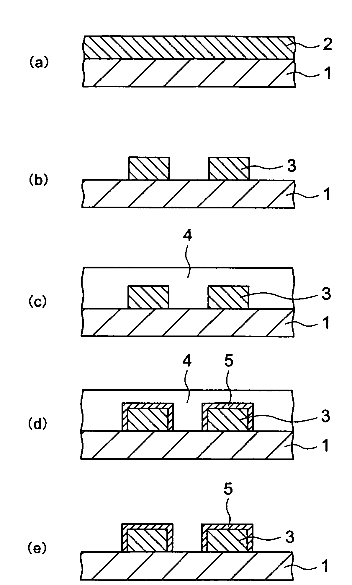
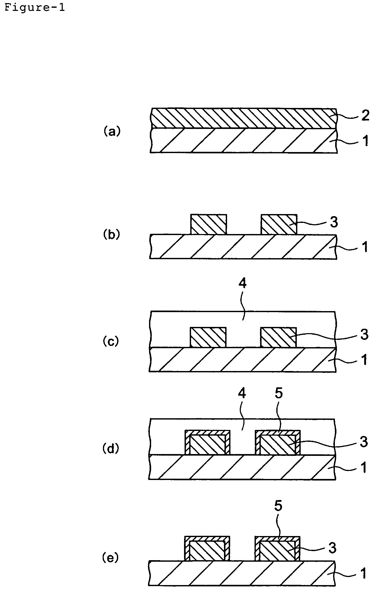
Image

Examples
example-1
(Preparation of Fine Pattern Forming Material)
[0038]100 parts by weight of polyvinyl acetal (acetylization degree: 12 mol %, acetalization degree: 30 mol %), 20 parts by weight of a water-soluble crosslinking agent of a urea derivative (methoxymethyl imidazolidinone) and 4 parts by weight of tetramethylammonium hydroxide (TMAH) were solved in 1470 parts by weight of a mixed solvent of pure water and isopropyl alcohol which is a water-soluble organic solvent (5 parts by weight of isopropyl alcohol relative to 95 parts by weight of pure water), to prepare the fine pattern forming material A (Composition A). The pH value thereof was 8.8. Next, Composition A was put into the following “Inspection for a film thickness of a coated layer” and “Inspection for development defects”.
(Inspection for a Film Thickness of a Coated Layer)
[0039]AZ KrF-17B 80 (manufactured by Clariant Co. AZ is a registered trademark, the followings are the same.) was spin-coated on a 6-inch bare silicon wafer, follo...
example-2
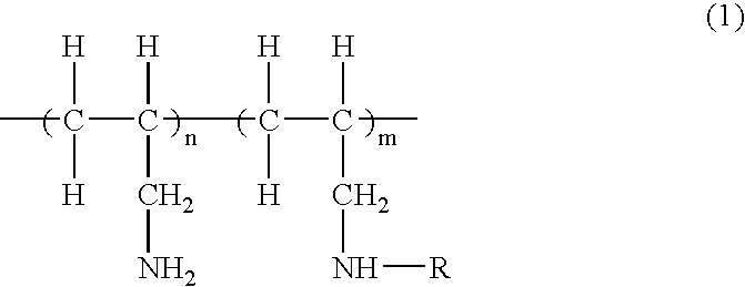
[0041]Except using partially methoxy carbonylated polyallylamine (PAA) represented by the general formula (2) below (n=50, m=50, average molecular weight: 3000) in place of TMAH, the same manner was carried out as Example-1 to prepare a fine pattern forming material B (Composition B). The pH value thereof was 7.3. “Inspection for a film thickness of a coated layer” and “Inspection for development defects” were carried out in the same manner as Example-1. The result is shown in Table 1.
[0042]
example-3
[0043]Except using partially methoxy carbonylated polyallylamine represented by the general formula (2) above (n=50, m=50, average molecular weight: 5000) in place of TMAH, the same manner was carried out as Example-1 to prepare a fine pattern forming material C (Composition C). The pH value thereof was 7.3. “Inspection for a film thickness of a coated layer” and “Inspection for development defects” were carried out in the same manner as Example-1. The result is shown in Table 1. Composition C was put into the following “Evaluation for coatability”.
(Evaluation for Coatability)
[0044]Composition C was output on an 8-inch bare silicon wafer by 5, 7.5 and 10 cc, spin-coated at 3500 rpm and baking on a direct hotplate at 85° C. for 70 seconds to form a film of a radiation sensitive resin composition for forming a fine pattern. At this time minimum output volume was gained by observing whether or not the coating reached to an edge of the wafer evenly. The result is shown in Table-2.
PUM
| Property | Measurement | Unit |
|---|---|---|
| temperature | aaaaa | aaaaa |
| mol % | aaaaa | aaaaa |
| temperature | aaaaa | aaaaa |
Abstract
Description
Claims
Application Information