
Solar Cell Comprising a Plasmonic Back Reflector and Method Therefor

a solar cell and back reflector technology, applied in the field of photovoltaic devices, can solve the problems of limited adoption of solar cell technology, inefficient energy converters of solar cells, and high manufacturing costs, and achieve the effect of improving energy conversion efficiency and light absorption

Inactive Publication Date: 2012-05-24
THE BOARD OF TRUSTEES OF THE LELAND STANFORD JUNIOR UNIV
View PDF23 Cites 19 Cited by
  • Summary
  • Abstract
  • Description
  • Claims
  • Application Information

AI Technical Summary

Benefits of technology

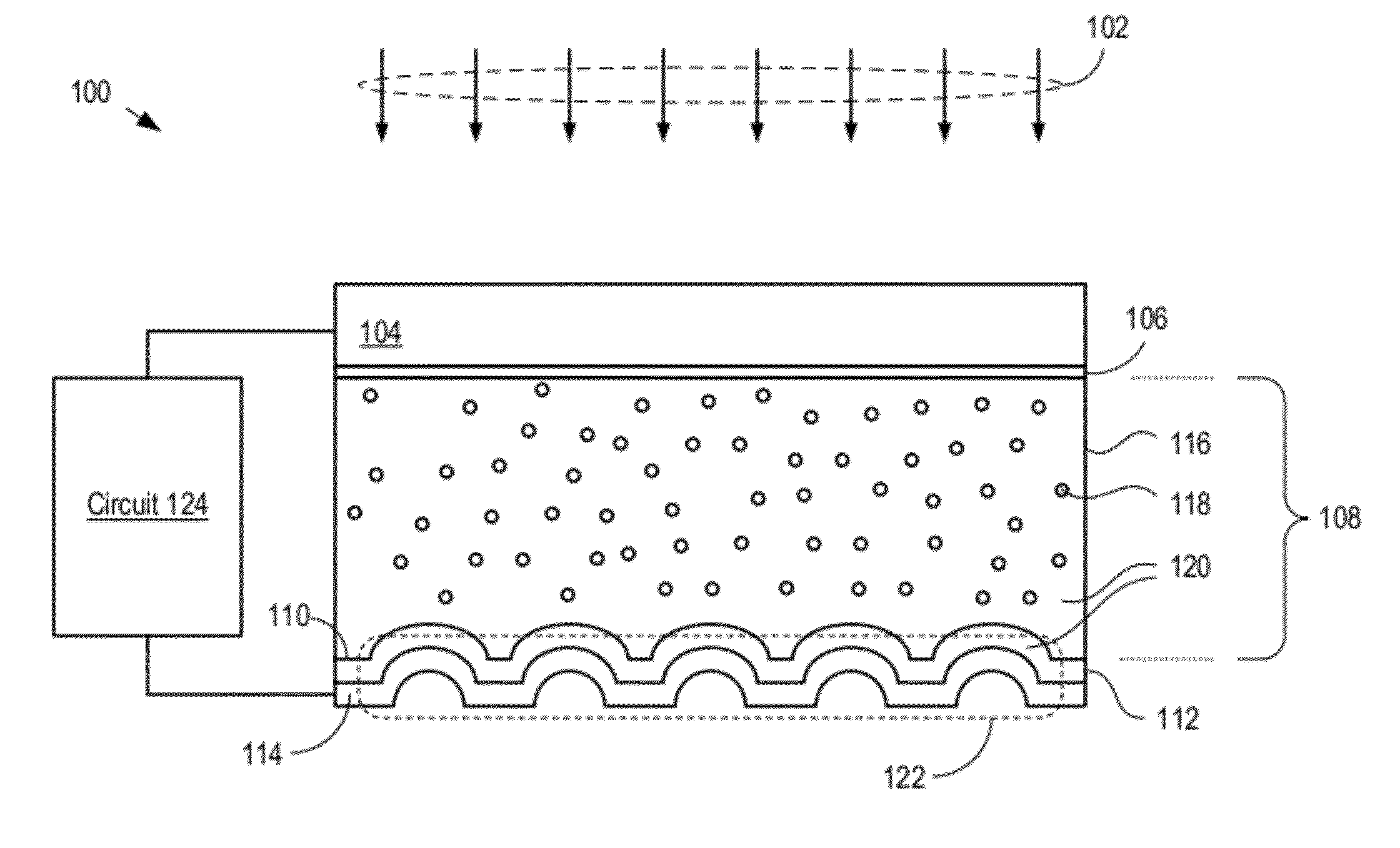
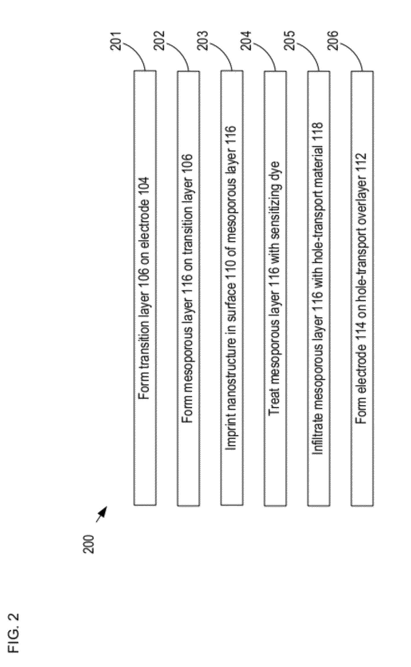
The present invention provides a solid-state dye-sensitized solar cell that overcomes some of the costs and disadvantages of prior art. The cell includes a plasmonic back reflector with a surface that is corrugated with a two-dimensional arrangement of nanometer-scale features. These features enable plasmonic effects that improve light absorption in the active layer of the cell and, thus, its energy-conversion efficiency. The cell can be used in energy conversion systems, solar panels, and portable power supplies. The invention also includes a method for fabricating the solar cell that includes operations where an active layer is nanoimprinted to form a surface with corrugated features, which are then coated with a sensitizing dye and infiltrated with hole-transport material to form a conformal overlayer of hole-transport material. The active layer comprises a mesoporous layer of titanium dioxide coated with a sensitizing dye. The invention also includes a plasmonic surface that is formed by the arrangement of surface features on the electrode.

Problems solved by technology

Unfortunately, solar cells tend to be inefficient energy converters and quite expensive to manufacture.
As a result, the cost to generate electrical energy using conventional solar cells has not been competitive with fossil-fuel-based energy generation, which has limited the adoption of solar-cell technology.
Unfortunately, DSCs comprising liquid electrolytes have several drawbacks, including leakage of the electrolyte, and electrolyte volatility.
Further, liquid electrolytes are typically corrosive, making them difficult to work with in a fabrication environment.
Conventional solid-state DSCs are not without problems, however.
First, electron-hole recombination in the devices leads to reduced energy-conversion efficiency.
Second, the hole-transport material tends to fill the pores of the porous titanium dioxide layer incompletely when applied.
These factors combine to limit the practical thickness for ss-DSCs to only about two microns.
This thickness is significantly less than the thickness desired for efficient light absorption in the active layer.
The resultant poor light absorption further reduces the energy-conversion efficiency of ss-DSCs.
Such efforts have had limited success in improving the overall energy-conversion efficiency of ss-DSCs, however.

Method used


Image

  • Solar Cell Comprising a Plasmonic Back Reflector and Method Therefor
  • Solar Cell Comprising a Plasmonic Back Reflector and Method Therefor
  • Solar Cell Comprising a Plasmonic Back Reflector and Method Therefor

Examples


Embodiment Construction

[0034]The following terms are defined for use in this Specification, including the appended claims:[0035]Disposed on or Formed on is defined as “exists on” an underlying material or layer. This layer may comprise intermediate layers, such as transitional layers, necessary to ensure a suitable surface. For example, if a material is described to be “disposed (or grown) on a substrate,” this can mean that either (1) the material is in intimate contact with the substrate; or (2) the material is in contact with one or more layers that interpose the material and the substrate.[0036]Nanoimprinted surface is defined as a surface having proactively created surface structure that has dimensions within the range of approximately 1 nm to 1000 nm, and which is created via nanoimprint lithography techniques, such as hard nanoimprint lithography or soft nanoimprint lithography.[0037]Plasmonic surface is defined as a surface comprising nanometer-scale surface features that collectively support the ...


PUM

PropertyMeasurementUnit
thicknessaaaaaaaaaa
thicknessaaaaaaaaaa
widthaaaaaaaaaa

Abstract

A method for forming a solar cell having a plasmonic back reflector is disclosed. The method includes the formation of a nanoimprinted surface on which a metal electrode is conformally disposed. The surface structure of the nanoimprinted surface gives rise to a two-dimensional pattern of nanometer-scale features in the metal electrode enabling these features to collectively form the plasmonic back reflector.

Description

CROSS REFERENCE TO RELATED APPLICATIONS[0001]This case is a continuation-in-part of co-pending U.S. patent application Ser. No. 12 / 909,064 (Applicant Docket: 146-019us), entitled “Optoelectronic Semiconductor Device and Method of Fabrication,” filed Oct. 21, 2010, which claims the benefit of U.S. Provisional Application Ser. No. 61 / 254,513, filed Oct. 23, 2009, entitled “Optoelectronic Semiconductor Device and Method of Fabrication” (Attorney Docket: 146-016US) and U.S. Provisional Application Ser. No. 61 / 263,582, filed Nov. 23, 2009, entitled “Substrate Comprising a Nanometer-scale Projection Array,” (Attorney Docket: 146-017US). This application also claims priority of provisional patent application U.S. Ser. No. 61 / 458,678, filed Nov. 29, 2010 (Attorney Docket S10-299 / PROV). The entire contents of each of these cases are incorporated herein by reference.[0002]If there are any contradictions or inconsistencies in language between this application and one or more of the cases that ...

Claims


Application Information

Patent Timeline
Patent Type & Authority Applications(United States)
IPC IPC(8): H01L31/0224H01L31/18H10K99/00
CPCB82Y20/00Y02E10/542Y02E10/549H01G9/2031H01L2251/105H01G9/209H01L51/0096H01L51/4226H01L51/447H01G9/2059Y02P70/50H10K77/10H10K30/151H10K30/87H10K71/821H10K30/50
Inventor DING, I-KANGZHU, JIACUI, YIMCGEHEE, MICHAEL DAVID
Owner THE BOARD OF TRUSTEES OF THE LELAND STANFORD JUNIOR UNIV
Learn More