Semiconductor sensor

a technology of semiconductor wafers and sensors, applied in the direction of microstructural devices, semiconductor/solid-state device details, coatings, etc., can solve the problems of insufficient protection of the protective layer from the moving portion, damage to the chips, adversely affecting the electrodes in electrical and mechanical connection, etc., to achieve the effect of improving the workability and throughput of detaching the semiconductor wafer from the jig

Inactive Publication Date: 2005-07-21
DENSO CORP
View PDF25 Cites 37 Cited by
  • Summary
  • Abstract
  • Description
  • Claims
  • Application Information

AI Technical Summary

Benefits of technology

[0013] To solve the problem described above, according to the present invention, the protective sheet and the semiconductor wafer are detached from the jig by a pressure applied to the protective sheet from a side of the jig. Accordingly, the semiconductor wafer can be detached without being damaged together with the protective sheet. Workability and throughput for detaching the semiconductor wafer from the jig are also improved.
[0014] Further, to solve the problem describe above, according to another aspect of the present invention, a wafer detachment device is used for detaching the semiconductor wafer and the protective sheet from the jig. The wafer detachment device has the jig for fixedly holding the protective sheet, and pressurizing means for applying a pressure to the protective sheet. Accordingly, the protective sheet is detached from the jig by the pressure together with the semiconductor device readily.

Problems solved by technology

In the conventional method described above, however, because the protective sheet is diced together with the semiconductor wafer, scraps of the protective sheet such as adhesive organic particles are produced by cutting and attached to the chips as contaminants.
The scraps may be attached to electrodes formed on each chip to adversely affect the electrodes in electrical and mechanical connection.
If the protective sheet is bonded to the semiconductor wafer firmly, the removal of the protective sheet is difficult and may cause damages to the chips by a stress.
As a result, the protective layer cannot protect the movable portions sufficiently.

Method used


Image

  • Semiconductor sensor
  • Semiconductor sensor
  • Semiconductor sensor

Examples


first embodiment

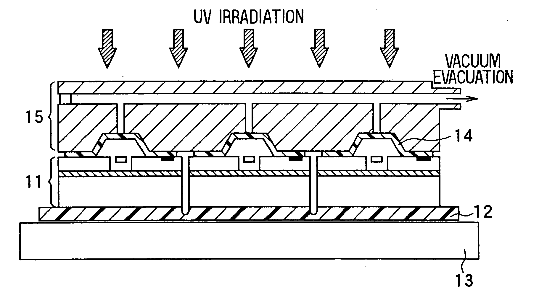
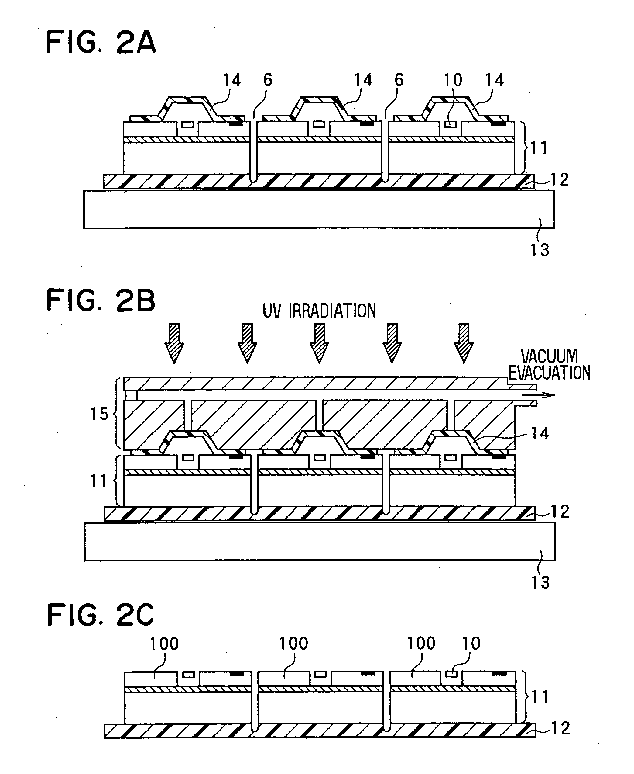
[0031] In a first preferred embodiment, a method for producing a semiconductor device according to the present invention is applied to various semiconductor devices including movable portions such as a surface micro-processed type acceleration sensor, a rotation angle sensor, and a reflecting digital micro-mirror projector (DMD). The method in the first embodiment is explained referring to FIGS. 1A to 1E and 2A to 2C.

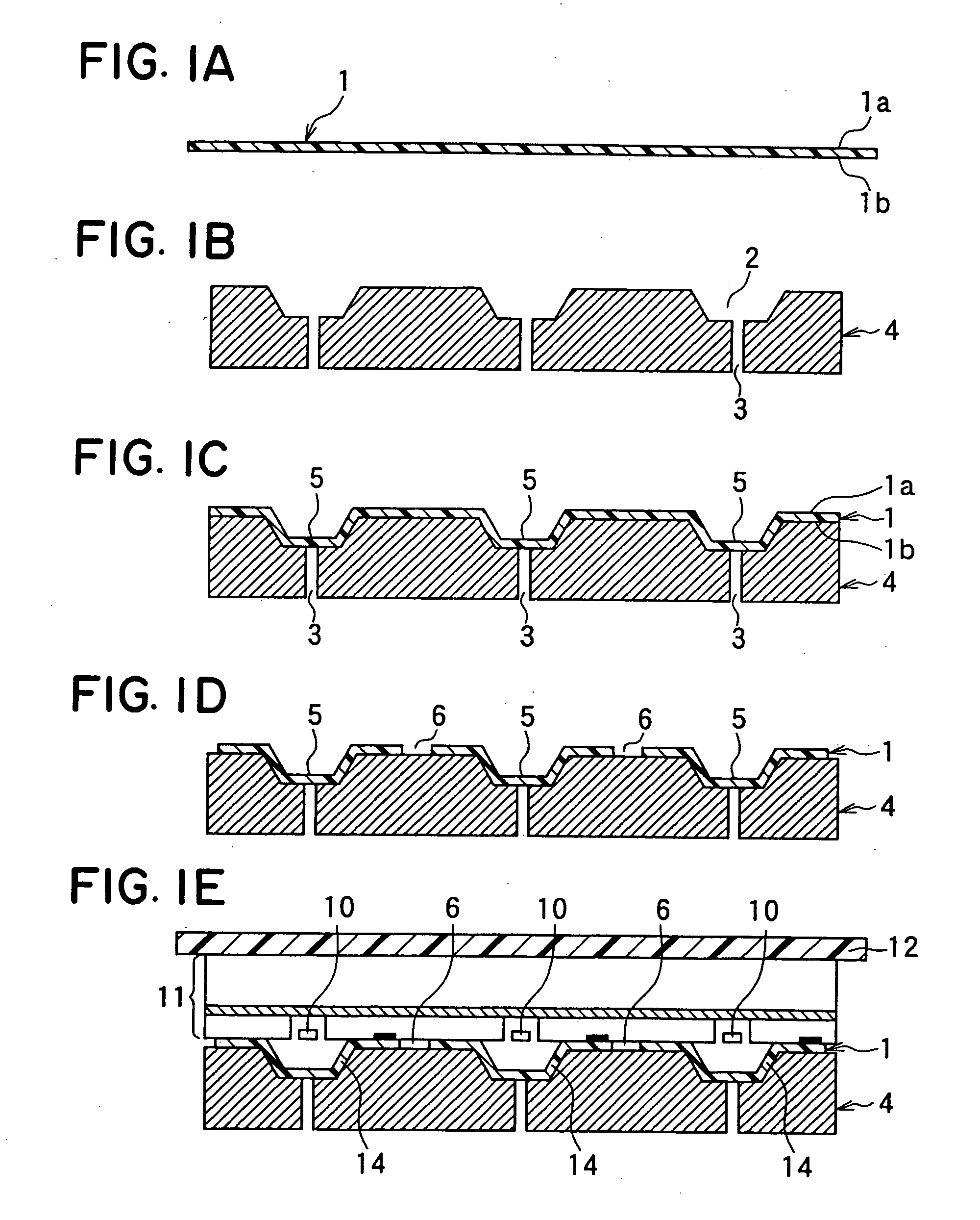
[0032] First, as shown in FIG. 1A, a protective sheet 1 is prepared. The protective sheet 1 is formed from an UV-setting adhesive sheet, a base of which is made of, for example, polyolefine. The protective sheet 1 has an adhesive surface la for covering a semiconductor wafer 11, and a surface 1b at an opposite side of the adhesive surface 1a. Further, a jig 4 shown in FIG. 1B is disposed on a heater block (not shown). The jig 4 has recesses 2 and holes 3 for vacuum absorption. The heater block performs the vacuum absorption in cooperation with the holes 3 of the jig 4....

second embodiment

[0043] In a second preferred embodiment, the protective members (protective caps) 14 are formed similarly to the first embodiment. Differences from the first embodiment are that the semiconductor wafer 11 has pad portions 21 for being electrically connected to external circuits by wire bonding (see FIG. 3E), and that the protective members 14 are not removed and remain in products. Therefore, the protective members 14 need to be partially removed at portions corresponding to the pad portions 21. The main differences from the first embodiment are described in more detail below. It should be noted that the same parts as those in the first embodiment are assigned to the same reference numerals in the second embodiment and other embodiments described below.

[0044]FIGS. 3A to 3E, 4A, and 4B schematically show the method for producing the semiconductor device in the second embodiment in a stepwise manner. The steps shown in FIGS. 3A, 3B and3C are performed in substantially the same manner...

third embodiment

[0050]FIGS. 8A to 8F show a method for producing a semiconductor device in a stepwise manner in a third preferred embodiment. In the first and second embodiments, the semiconductor wafer 11 is processed from one surface thereof. To the contrary, in the present embodiment, the semiconductor wafer 11 is processed from front and back surfaces thereof. That is, as shown in FIG. 8A, the semiconductor wafer 11 in the present embodiment has back surface processed portions 41 formed as opening portions by etching or the like performed from the back surface. The movable portions 10 are exposed from both front and back surfaces of the semiconductor wafer 11.

[0051] At a back side adhesive sheet bonding step, an adhesive sheet (back side protective sheet) 42 is bonded to the back surface of the semiconductor wafer 11 to protect the back surface. Further, at the wafer bonding step, the protective sheet 1, which is processed as in the first embodiment to have the grooves 6, is bonded to the fron...


PUM

PropertyMeasurementUnit
temperatureaaaaaaaaaa
thicknessaaaaaaaaaa
depthaaaaaaaaaa

Abstract

A protective sheet is fixed to a jig, and regions of the protective sheet corresponding to regions where dicing-cut is to be performed are removed to form grooves. Then, a semiconductor wafer is bonded to the protective sheet at an opposite side of the jig, and the jig is detached from the protective sheet and the semiconductor wafer bonded together. After that, the semiconductor wafer is cut into semiconductor chips by dicing along the grooves of the protective sheet. Because the protective sheet is not cut by dicing, no scraps of the protective sheet is produced, thereby preventing contamination to the chips.

Description

CROSS REFERENCE TO RELATED APPLICATIONS [0001] This application is based upon and claims the benefit of Japanese Patent Applications No. 11-76566 filed on Mar. 19, 1999, and No. 11-196345 filed on Jul. 9, 1999, the contents of which are incorporated herein by reference. BACKGROUND OF THE INVENTION [0002] 1. Field of the Invention [0003] This invention relates to a method for producing a semiconductor device by dicing a semiconductor wafer covered with a protective sheet along scribe lines, a semiconductor device produced by the method, and a wafer detachment apparatus usable for the method. [0004] 2. Description of the Related Art [0005] As disclosed in many documents such as JP-A-10-242253, JP-A-7-99172, U.S. Pat. No. 5,824,177, and U.S. Pat. No. 5,362,681, when a semiconductor wafer having plural movable portions is divided into plural chips, a protective sheet is attached to the semiconductor wafer to protect the movable portions. In this state, the semiconductor wafer is diced i...

Claims


Application Information

Patent Timeline
Patent Type & Authority Applications(United States)
IPC IPC(8): B81C1/00H01L21/301H01L21/68
CPCB29C33/0022B29C2043/023H01L2924/10253H01L2224/45124H01L2224/45144H01L2924/01322H01L2924/01068B81C1/00888B81C1/00896B81C2201/053H01L21/6836H01L2221/68327H01L2224/16H01L2224/48095H01L2224/73265H01L2924/01057H01L2924/01079H01L2924/09701H01L2924/30105H01L2924/00H01L2924/00014H01L2224/48465H01L2924/16235
Inventor FUJII, TETSUOFUKADA, TSUYOSHIAO, KENICHI
Owner DENSO CORP
Why Eureka
Try Eureka