Active matrix display device

a display device and active matrix technology, applied in the direction of identification means, digital storage, instruments, etc., can solve the problems of deteriorating device performance, difficult to precisely control the operation of the seventh transistor, and may no longer drive the lcd, so as to prevent the degradation of the shift register, improve the picture quality, and improve the life span

Active Publication Date: 2005-07-21
LG DISPLAY CO LTD
View PDF13 Cites 68 Cited by
  • Summary
  • Abstract
  • Description
  • Claims
  • Application Information

AI Technical Summary

Benefits of technology

[0025] An object of the present invention is to provide an active matrix display device capable of preventing degradation of a shift register to improve its life span and improve picture quality.

Problems solved by technology

If the degradation of the seventh transistor T7 is serious, the seventh transistor T7 can be fatally damaged, so that the LCD may no longer be driven.
The device performance can deteriorate so much that it becomes difficult to precisely control the operation of the seventh transistor T7.
As a result, a desired image is not displayed on the LCD screen.
Also, the degradation of the seventh transistor results in a shortening of the life span for the LCD.

Method used


Image

  • Active matrix display device
  • Active matrix display device
  • Active matrix display device

Examples


first embodiment

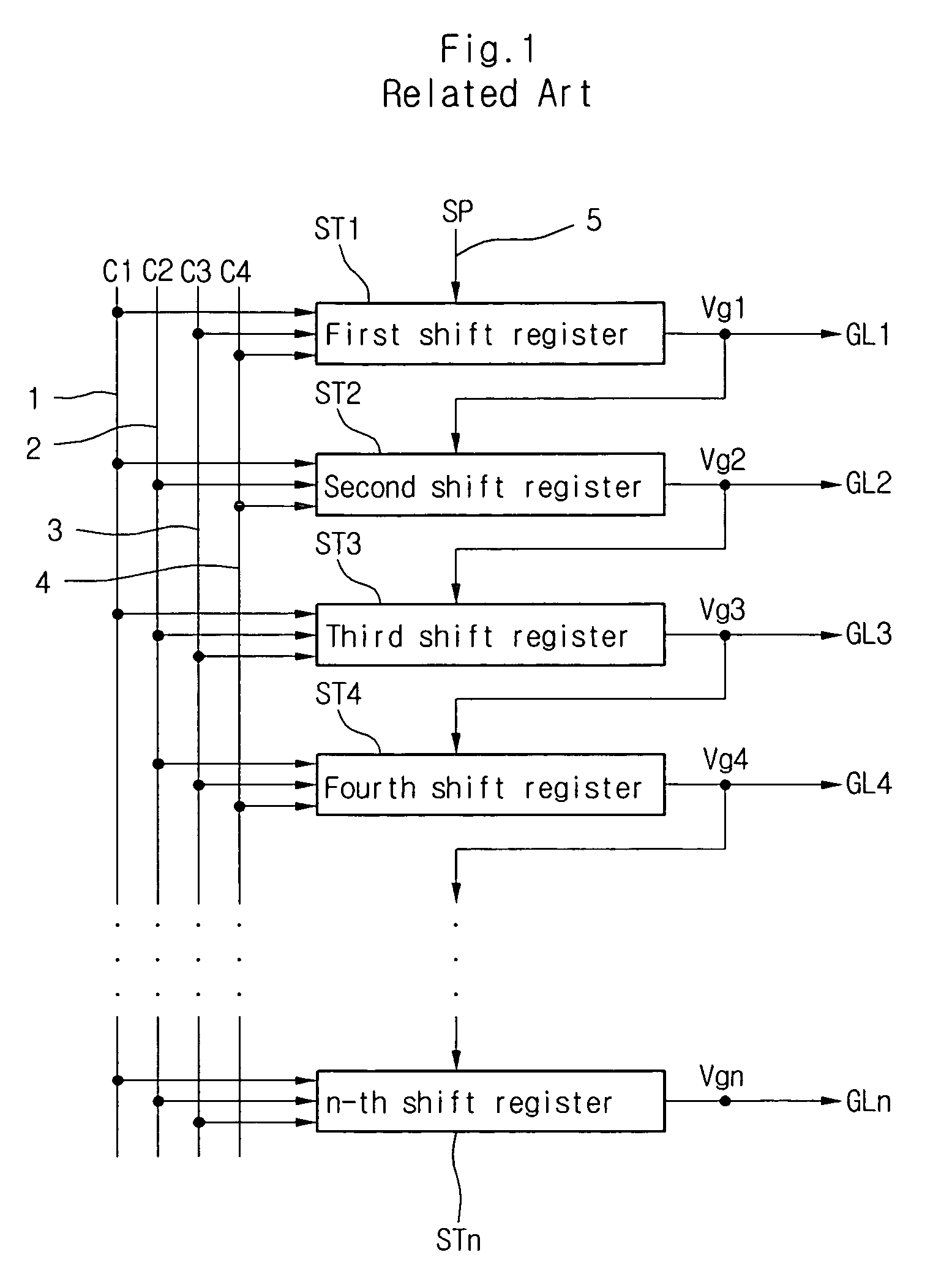
[0045]FIG. 5 is a circuit diagram illustrating a shift register of a gate driver in an LCD according to the present invention. A gate driver of an LCD includes a plurality of shift registers for supplying output signals Vg1 to Vgn in sequence. A description will be made with reference to a first shift register ST1 among the shift registers ST1 to STn. The remaining shifter registers ST2 to STn operate in a somewhat similar manner as the first shifter register ST1. A high-state voltage output signal Vg1 of the first shift register ST1 is supplied as a start pulse to the second shift register ST2, and a high-state voltage output signal Vg2 from the second shift register ST2 is supplied as a start pulse to the third shift register ST3. In the same manner, the remaining shift registers ST4 to STn receive high-state voltage output signals from previous stages as their start pulses and produce high-state voltage output signals whose phases are shifted so as to follow one after another.

[00...

second embodiment

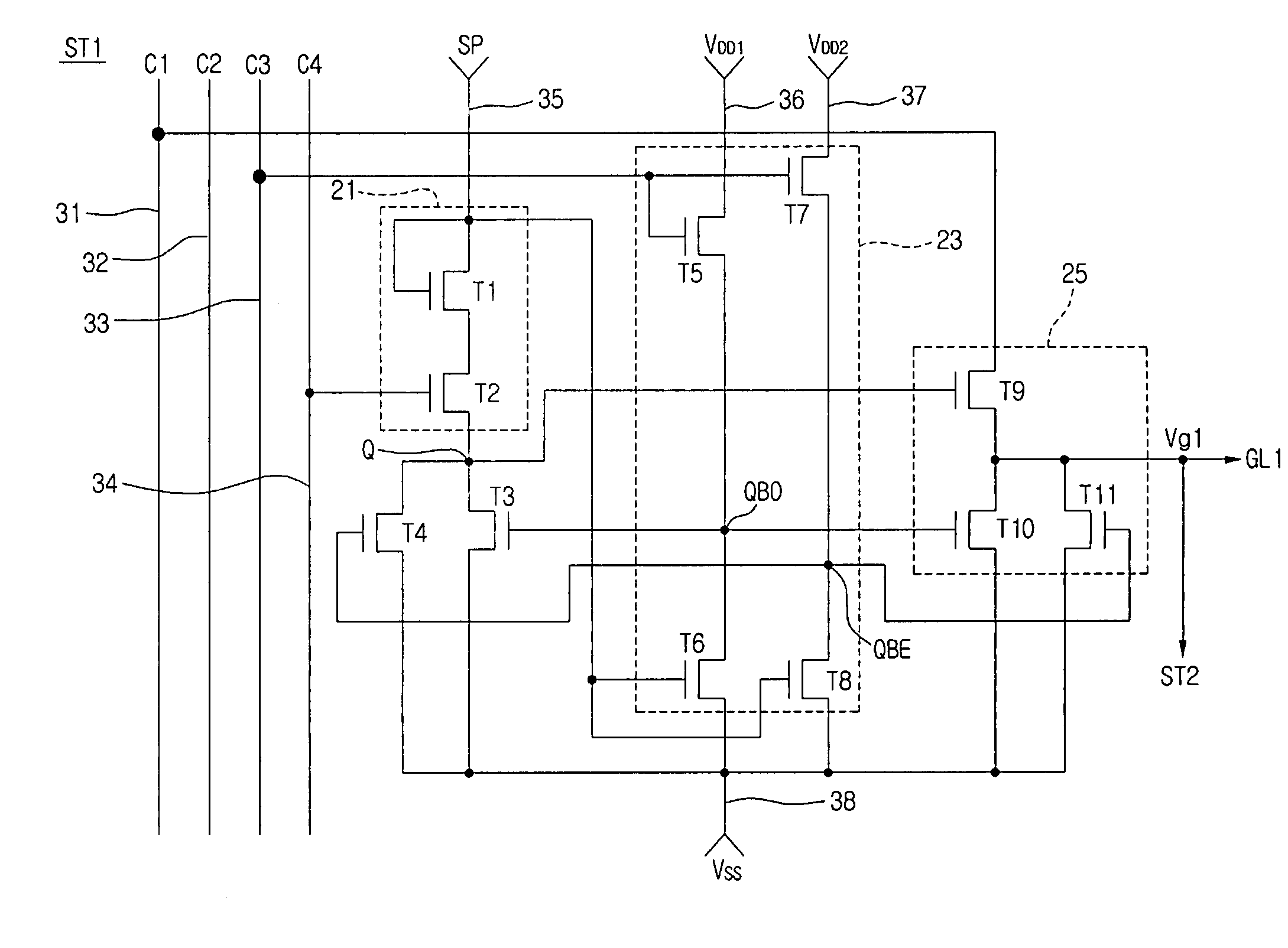
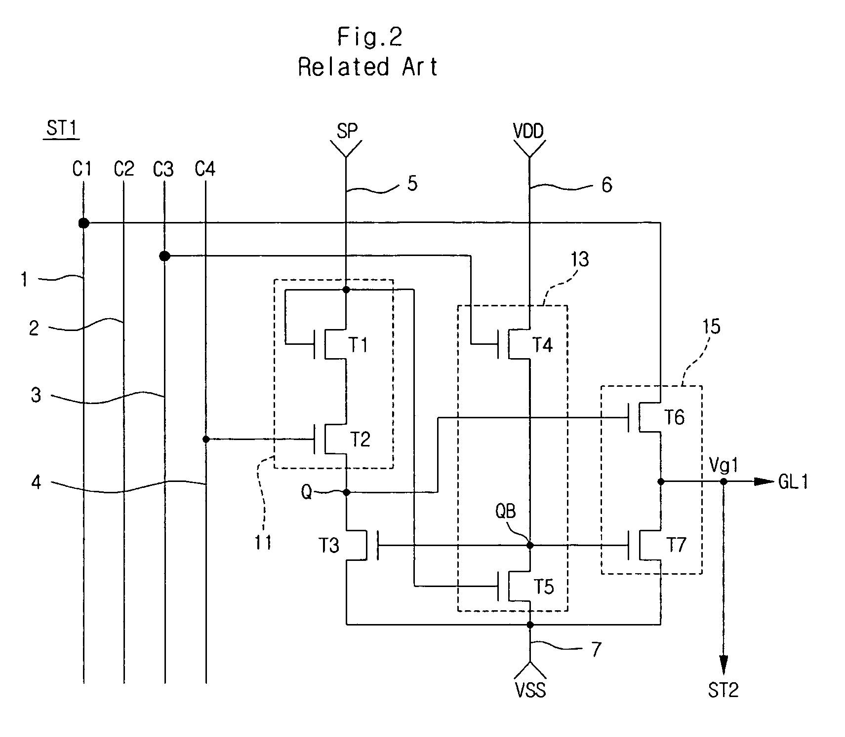
[0077]FIG. 9 is a circuit diagram illustrating a shift register of a gate driver in an LCD according to the present invention. Referring to FIG. 9, a first control part 21 and an output part 25 are similar to those shown in FIG. 5. Only the second control part 23 is different from the second control part of FIG. 5. Therefore, the following description will be made centering on the second control part 23.

[0078] The second control part 23 controls the nodes QBO and QBE to output the first supply voltage VSS through a tenth or eleventh transistor T10 or T11 of the output part 25. The first supply voltage VSS is supplied as the output voltage Vg1 at a low-state voltage through the first gate line GL1. For this purpose, the second control part 23 includes: a fifth transistor T5 coupled to a second supply voltage (VDD1) input line 36, a third clock signal (C3) input line 33, and the node QBO; a sixth transistor T6 coupled to the node QBO, a start pulse (SP) input line 35, and a first supp...

third embodiment

[0090] In this case, the time necessary for the high-state voltage supplied to the node Q to change to the first supply voltage VSS is delayed somewhat due to the characteristic of the node Q. In order to reduce the time delay occurring at the node Q, the third embodiment further includes the fourteenth transistor T14. That is, if the third clock signal C3 becomes a high-state voltage in the fourth period, the fifth and seventh transistors T5 and T7 are turned on at the same time and the fourteenth transistor T14 is also turned on in response to the third clock signal C3.

[0091] Then, the second supply voltage VDD1 at a high-state voltage is supplied to the node QBO due to the turned-on fifth transistor T5, and the third and tenth transistors T3 and T10 are turned on in response to the second supply voltage VDD1 at a high-state voltage at the same time. At this time, the first supply voltage VSS of a low-state voltage is supplied to the node Q due to the third transistor T3. Also, th...


PUM

PropertyMeasurementUnit
voltage swingaaaaaaaaaa
voltageaaaaaaaaaa
voltageaaaaaaaaaa

Abstract

An active matrix display device includes: a display panel having gate lines and data lines defining pixels; a gate driver in the display panel to supply output signals to gate lines of the display panel; and a data driver to supply image signals to data lines of the display panel, wherein the gate driver includes a plurality of shift registers to output signals that are sequentially shifted, each of the shift registers including: a first control part for controlling a first node in response to a first clock signal among a plurality of clock signals; a second control part for controlling second and third nodes in response to the start signal and a second clock signal; and an output part to selectively output one of a third clock signal and a first supply voltage in response to voltages of the first, second, and third nodes, whereby second and third supply voltages, which are different from each other, are switched for application at the second and third nodes.

Description

[0001] The present invention claims the benefit of Korean Patent Application No. 2003-99481 filed in Korea on Dec. 30, 2003, which is hereby incorporated by reference. BACKGROUND OF THE INVENTION [0002] 1. Field of the Invention [0003] The present invention relates to an active matrix display device, and more particularly, to an active matrix display device capable of preventing degradation. [0004] 2. Description of the Related Art [0005] In general, display devices, such as liquid crystal displays (LCDs) or organic light emitting diodes (OLEDs), that display images by driving pixels arranged in an active matrix configuration are actively researched. In particular, the LCD displays desired images by supplying data voltages corresponding to image information to pixels arranged in the active matrix configuration to adjust light transmittance through the liquid crystal layer. For this purpose, the LCD is provided with a liquid crystal panel having pixels arranged in a matrix configurat...

Claims


Application Information

Patent Timeline
Patent Type & Authority Applications(United States)
IPC IPC(8): G09G3/36G02F1/133G02F1/136G09F9/00G11C19/00G11C19/28H01L29/786
CPCG09G3/3677G11C19/28G11C19/00G09G3/36
Inventor JANG, YONG HOCHO, NAM WOOKYOON, SOO YOUNG
Owner LG DISPLAY CO LTD
Why Eureka
Try Eureka