Printed circuit board and method for manufacturing printed circuit board

a printed circuit board and printed circuit technology, applied in the direction of printed circuit non-printed electric components association, sustainable manufacturing/processing, final product manufacturing, etc., can solve the problems of small behavior of capacitors incorporated cracks and peelings that cannot be easily detected in the core substrate, etc., to achieve the effect of preventing generation of migration, increasing the connection between the via hole and the electrode, and broadening the alignment rang

Inactive Publication Date: 2005-07-21
IBIDEN CO LTD
View PDF18 Cites 56 Cited by
  • Summary
  • Abstract
  • Description
  • Claims
  • Application Information

AI Technical Summary

Benefits of technology

[0011] In the invention recited in claim 1, a large cavity is formed in a core substrate, and a plurality of capacitors are accommodated in the cavity. With this arrangement, a plurality of capacitors can be reliably provided within the core substrate. The capacitors can be provided at places close to each other in the cavity, the package density of the capacitors can be increased. Since a plurality of capacitors are mounted within the cavity, the plurality of capacitors are aligned to the same heights with each other. A resin layer can be formed on the core substrate into a uniform thickness, and via holes can be stably formed. Since the cavity is formed in such a manner as to have a large area, the capacitors can be provided at accurate positions. As a result, an interlayer resin insulating layer and a conductor circuit can be properly formed on the core substrate, thereby lowering the rate of generating defective printed circuit boards.
[0157] In the invention recited in claim 78, a metal film is formed on the electrodes of the chip capacitors. As a result, the chip capacitor have a flat surface. When the chip capacitors are accommodated in the printed circuit board, and penetrating openings are formed in the resin which covers the electrodes, no resin is left. In this manner, the connection between the via holes and the electrodes has increased reliability.

Problems solved by technology

As a result, the behavior of the capacitors incorporated in the core substrate becomes small.
In this manner, even if internal stress is generated between the core substrate and the capacitors caused by the difference in the thermal expansion coefficients therebetween, cracks and peelings do not easily occur in the core substrate.

Method used


Image

  • Printed circuit board and method for manufacturing printed circuit board
  • Printed circuit board and method for manufacturing printed circuit board
  • Printed circuit board and method for manufacturing printed circuit board

Examples


first embodiment

[0231] Hereinafter, embodiments of the present invention will be described with reference to the drawings.

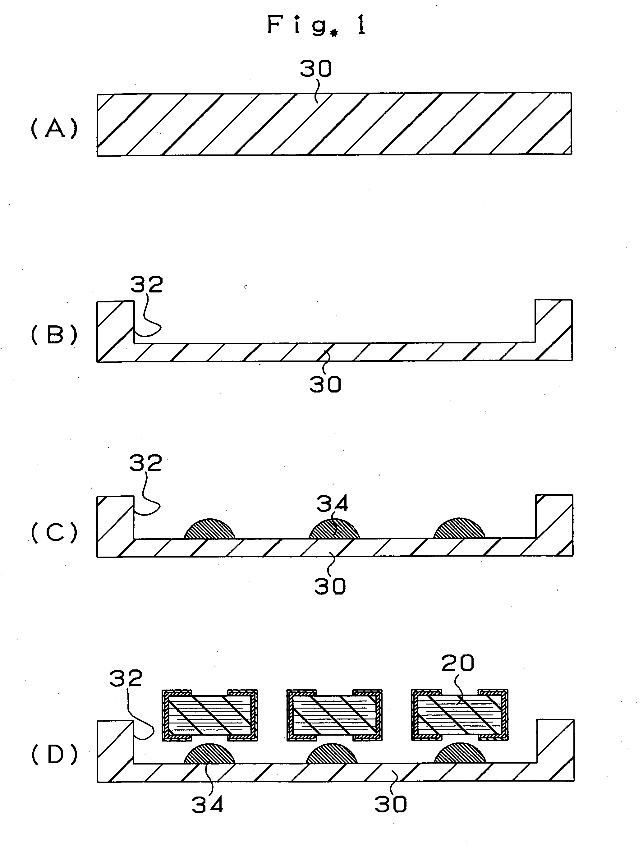
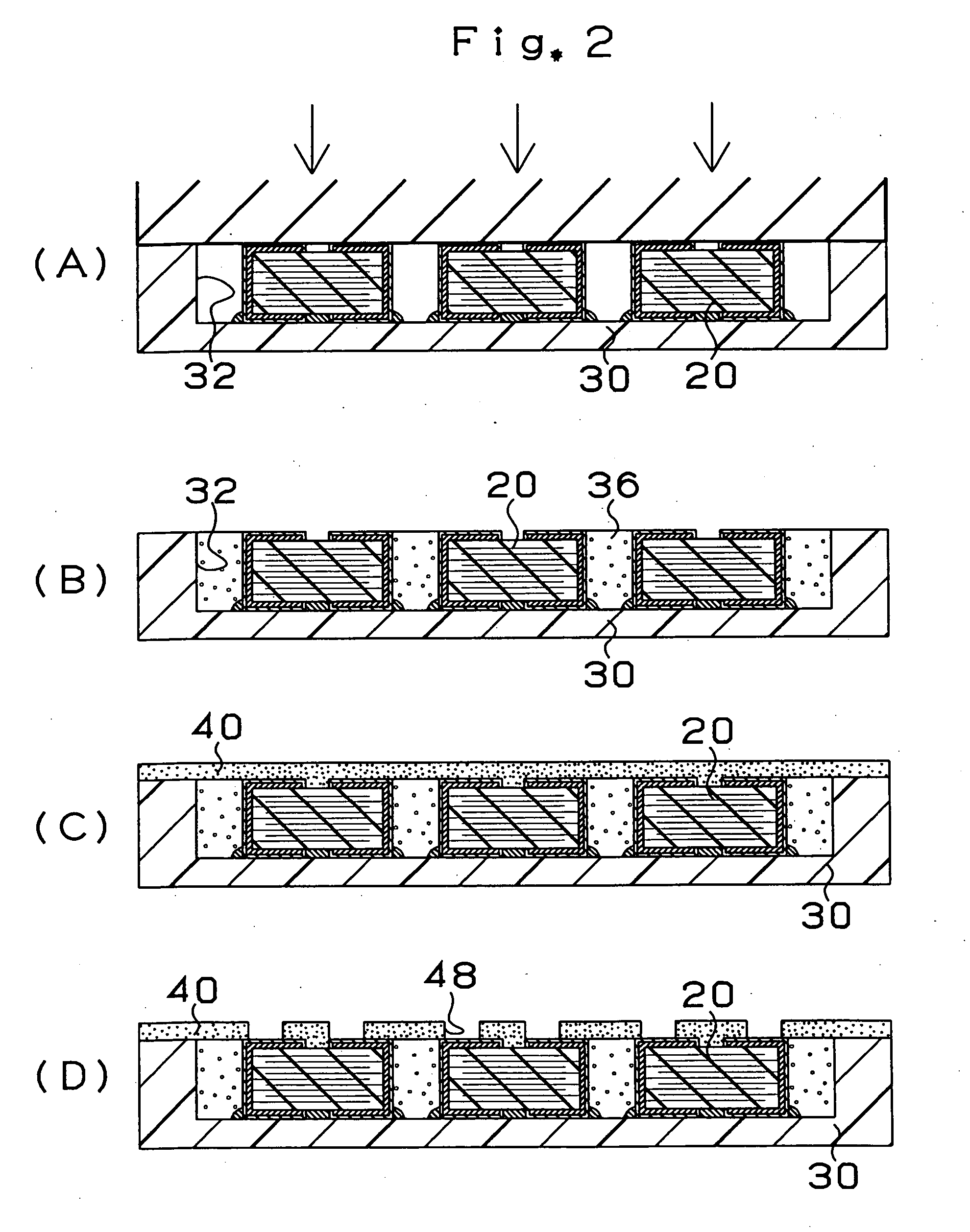
[0232] First, the structure of a printed circuit board according to a first embodiment of the present invention will be described with reference to FIGS. 7 and 8. FIG. 7 is a diagram showing a cross section of a printed circuit board 10. FIG. 8 is a diagram showing a state where an IC chip 90 is mounted on the printed circuit board 10 shown in FIG. 7, and the printed circuit board 10 is attached onto a daughter board 95.

[0233] As shown in FIG. 7, the printed circuit board 10 is constituted by a core substrate 30 accommodating a plurality of chip capacitors 20, and a buildup circuit layers 80A, 80B. The buildup circuit layers 80A and 80B are constituted by an interlayer resin insulating layer 50 and 150. The interlayer resin insulating layer 50 has via holes 160 and conductor circuits 158. The interlayer resin insulating layer 150 has via holes 161 and conductor circuits 159. A...

second embodiment

(Third Modification of Second Embodiment)

[0416] A printed circuit board according to a third modification of the second embodiment will be described with reference to FIG. 33. The printed circuit board according to the third modification has the similar structure as of the second embodiment, except for the following points. That is, in the printed circuit board according to the third modification, the first electrode 221, the second electrode 222 of the capacitor 220 are directly connected to the through hole 246 by a circuit pattern 257α provided between the accommodation layer 230a and the connection layer 240. In the third modification, the wire length from the first electrode 221 and the second electrode 222 to the daughter board can be shortened.

Fourth Modification of Second Embodiment

[0417] A printed circuit board according to a fourth modification of the second embodiment will be described with reference to FIG. 18.

[0418] The printed circuit board according to the fourth m...

third embodiment

[0441] First, the structure of a printed circuit board according to a third embodiment of the present invention will be described with reference to FIGS. 37 and 38. FIG. 37 is a diagram showing a cross section of a printed circuit board 410. FIG. 38 is a diagram showing the state where an IC chip 490 is mounted on the printed circuit board 410 shown in FIG. 37, and the printed circuit board 410 is attached to a daughter board 494.

[0442] As shown in FIG. 37, the printed circuit board 410 incorporates chip capacitors 420, a core substrate 430 for accommodating chip capacitors 420, and an interlayer resin insulating layer 450 constituting the buildup layers 480A, 480B. The core substrate 430 is constituted by an accommodating layer 430α for accommodating the capacitors 420, and a connection layer 440. Via holes 460 and a conductor circuit 458 are formed in the connection layer 440. Via holes 560 and a conductor circuit 558 are formed in the interlayer resin insulating layer 450. In th...


PUM

PropertyMeasurementUnit
temperatureaaaaaaaaaa
thicknessaaaaaaaaaa

Abstract

Chip capacitors 20 are provided in a printed circuit board 10. In this manner, the distance between an IC chip 90 and each chip capacitor 20 is shortened, and the loop inductance is reduced. In addition, the chip capacitors 20 are accommodated in a core substrate 30 having a large thickness. Therefore, the thickness of the printed circuit board does not become large.

Description

TECHNICAL FIELD [0001] The present invention relates to a printed circuit board on which electric elements, such as IC chips, are mounted. More specifically, the present invention relates to a printed circuit board incorporating capacitors therein, and a method for manufacturing the same. BACKGROUND ART [0002] In a computer, the length of electric wiring between the power supply and the IC chip is usually long, and therefore, the loop inductance at this electric wiring is extremely large. The variation in the voltage at which the IC is driven in high-speed operation mode becomes very large accordingly, possibly causing malfunction of the IC. In addition, it becomes difficult to stabilize the voltage of the power supply. In an attempt to avoid these troubles, a capacitor is mounted on the surface of the printed circuit board as an auxiliary device for assisting the power supply operation. [0003] Specifically, the loop inductance which causes the variation in voltage depends on the le...

Claims


Application Information

Patent Timeline
Patent Type & Authority Applications(United States)
IPC IPC(8): H01L21/48H01L23/498H01L23/50H01L23/64H01L25/16H05K1/02H05K1/18H05K3/46
CPCH01G4/224H05K1/183H01G4/40H01L21/4857H01L23/498H01L23/49822H01L23/49827H01L23/50H01L23/642H01L23/645H01L25/16H01L25/162H01L2224/16225H01L2224/16227H01L2224/16237H01L2924/01002H01L2924/01005H01L2924/01011H01L2924/01012H01L2924/01015H01L2924/01018H01L2924/0102H01L2924/01025H01L2924/01027H01L2924/01046H01L2924/01051H01L2924/01074H01L2924/01078H01L2924/01079H01L2924/14H01L2924/15174H01L2924/15192H01L2924/15311H01L2924/15312H01L2924/19041H01L2924/19105H01L2924/19106H01L2924/30107H01L2924/3011H05K1/0231H05K1/112H05K1/181H05K1/185H05K1/186H05K3/4602H05K2201/09509H05K2201/10636H05K2201/10674H01L2924/01019H01G4/228H01L2224/05573H01L2224/05568H01L2924/3511Y02P70/50H05K3/18H01L2224/05001H01L2224/05027H01L2224/05572H01L2224/05008H01L2224/05024H01G2/06H01G4/12H01G4/248H05K1/115H05K2201/09545H05K2201/096H05K2201/10015
Inventor INAGAKI, YASUSHIASAI, MOTOOWANG, DONGDONGYABASHI, HIDEOSHIRAI, SEIJI
Owner IBIDEN CO LTD
Why Eureka
Try Eureka