Substrate having film pattern and manufacturing method of the same, manufacturing method of semiconductor device, liquid crystal television, and EL television

a technology of film pattern and substrate, which is applied in the direction of photomechanical equipment, originals for photomechanical treatment, instruments, etc., can solve the problems of reducing throughput, affecting the effect of film pattern and resist, etc., to achieve the effect of reducing throughput, reducing wettability, and reducing wettability

Inactive Publication Date: 2005-07-21
SEMICON ENERGY LAB CO LTD
View PDF14 Cites 102 Cited by
  • Summary
  • Abstract
  • Description
  • Claims
  • Application Information

AI Technical Summary

Benefits of technology

[0010] The invention is made in view of the aforementioned problems to provide a manufacturing method of a substrate having a film pattern of an insulating film, a semiconductor film, a conductive film and the like through simple steps, and a manufacturing method of a low cost semiconductor device with high throughput and yield.
[0050] In this manner, according to the invention, a film pattern, a substrate having the film pattern, an insulating film having a contact hole, and moreover a semiconductor element and a semiconductor device having these can be formed through a simple process with high precision. Furthermore, the invention can provide a manufacturing method of a semiconductor element and a semiconductor device at low cost with high throughput and high yield.

Problems solved by technology

However, in the conventional process for forming a film pattern, an insulating film having a contact hole, and the like, bulk of materials of the film pattern and the resist are wasted and a large number of steps are required for forming a mask pattern, which decreases throughput.
In the case where the amount of application of resist and a surface condition of a base film are not controlled sufficiently when opening a contact hole, the resist spreads over the contact hole and a defective contact may occur.

Method used


Image

  • Substrate having film pattern and manufacturing method of the same, manufacturing method of semiconductor device, liquid crystal television, and EL television
  • Substrate having film pattern and manufacturing method of the same, manufacturing method of semiconductor device, liquid crystal television, and EL television
  • Substrate having film pattern and manufacturing method of the same, manufacturing method of semiconductor device, liquid crystal television, and EL television

Examples


embodiment mode 1

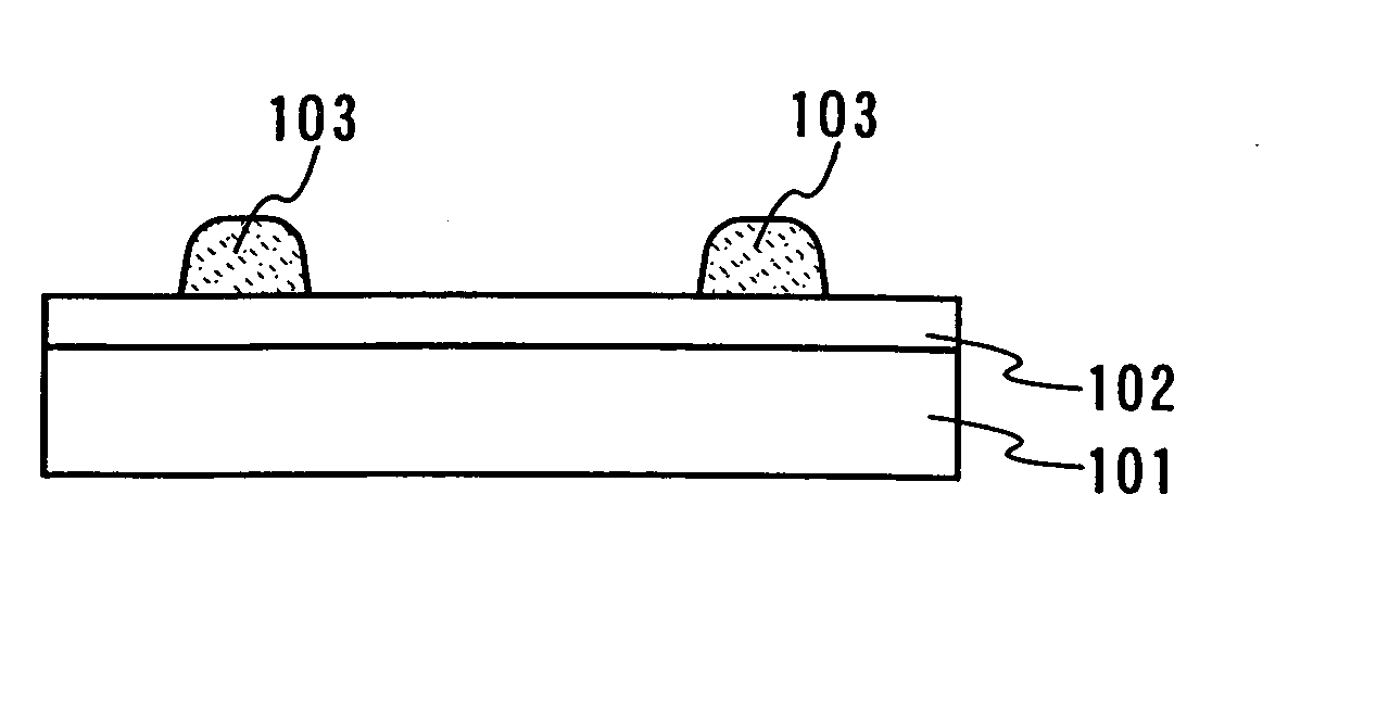
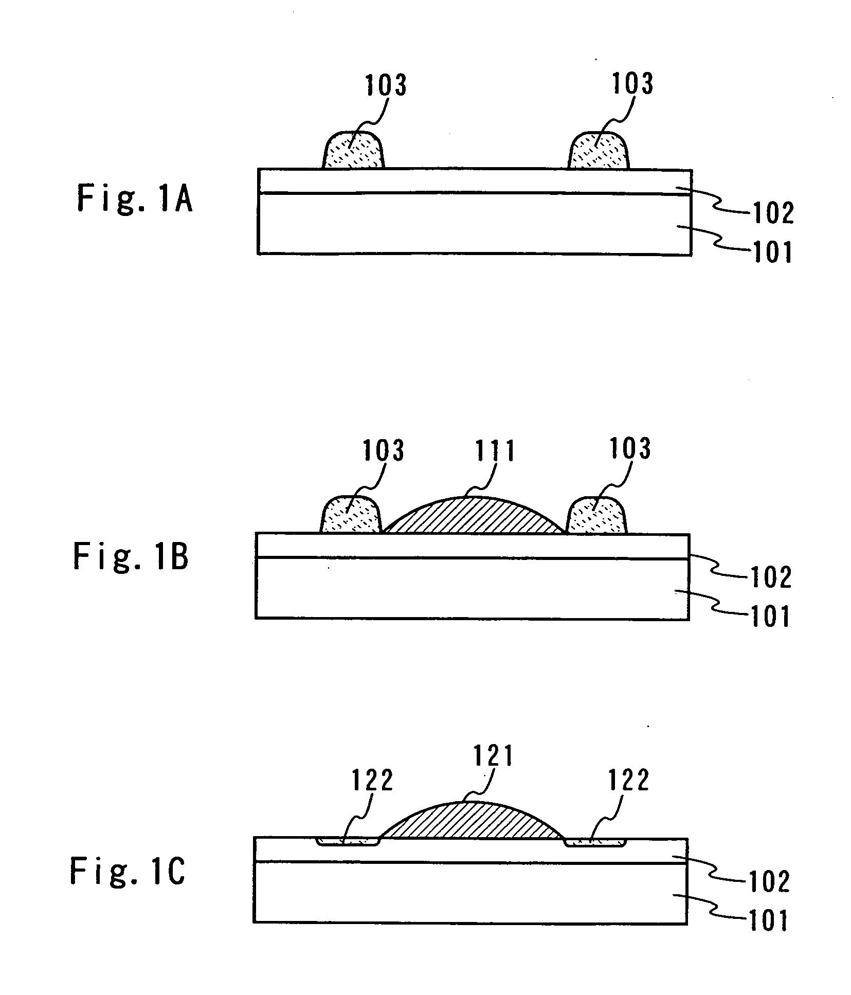
[0086] In this embodiment mode, a step for forming a film pattern having a desired shape by using a mask pattern which has low wettability is described with reference to FIG. 1. Note that the mask pattern described in this embodiment mode is a mask pattern used for forming a film pattern.

[0087] As shown in FIG. 1A, a first film 102 is formed on a substrate 101. A first mask pattern 103 which has low wettability is formed thereon by the droplet discharging method, the ink-jetting method and the like. Here, the droplet discharging method is used as a method for forming the mask pattern.

[0088] As the substrate 101, a glass substrate, a quartz substrate, a substrate formed of an insulating substance such as alumina, a plastic substrate which can resist a processing heat of a subsequent step, a silicon wafer, a metal substrate and the like can be used. In this case, it is preferable to form an insulating film for preventing impurities and the like from dispersing from a substrate side,...

embodiment mode 2

[0120] In this embodiment mode, steps for forming a film pattern having a desired shape by using a mask pattern formed of a material for forming a liquid repellent surface are described with reference to FIGS. 32A to 32C. Note that the mask pattern described in this embodiment is a mask pattern used for forming a film pattern.

[0121] As shown in FIG. 32A, a first film 1002 is formed on a substrate 1001. A protective film (first mask pattern) 1003 is formed thereon by the droplet discharging method, the ink-jetting method and the like. Here, the droplet discharging method is used for forming the mask pattern. It is preferable that the first film 1002 have a lyophilic surface. In the case where the substrate 1001 has a lyophilic surface, the first film is not required to be formed.

[0122] The substrate 1001 may be a glass substrate, a quartz substrate, a substrate formed of an insulating substance such as alumina, a plastic substrate which can resist the processing heat in a subsequen...

embodiment mode 3

[0136] The following embodiment modes and embodiments are described with reference to Embodiment Mode 1. However, Embodiment Mode 2 can be applied appropriately.

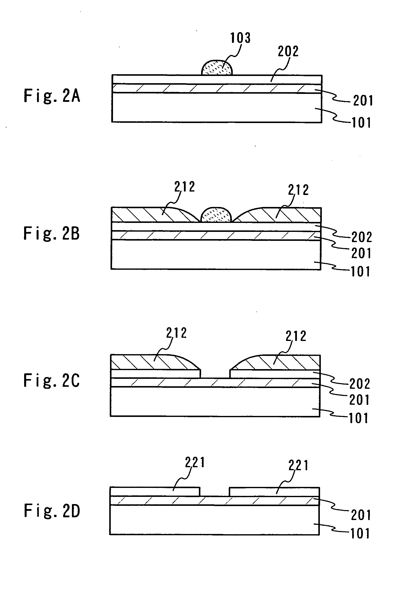
[0137] In this embodiment mode, steps of forming a film pattern having a desired shape using a first mask pattern which has low wettability and a second mask pattern which has high wettability is described with reference to FIGS. 2A to 2C. Note that the first mask pattern described in this embodiment mode is a mask pattern used for forming the second mask pattern. The second mask pattern is a mask pattern used for etching.

[0138] As shown in FIG. 2A, a first film 201 is formed on a first substrate 101 and a second film 202 is formed on the first film 201. An appropriate material is used for the first film. As the second film, a similar material to that of the first film 102 in Embodiment Mode 1 can be used.

[0139] Next, a first mask pattern 103 which has low wettability is formed on the second film 202 by applying a materia...


PUM

PropertyMeasurementUnit
contact angleaaaaaaaaaa
contact anglesaaaaaaaaaa

Abstract

The invention provides a manufacturing method of a substrate having a film pattern including an insulating film, a semiconductor film, a conductive film and the like by simple steps, and also a manufacturing method of a semiconductor device which is low in cost with high throughput and yield. According to the invention, after forming a first protective film which has low wettability on a substrate, a material which has high wettability is applied or discharged on an outer edge of a first mask pattern, thereby a film pattern and a substrate having the film pattern are formed.

Description

BACKGROUND OF THE INVENTION [0001] 1. Field of the Invention [0002] The present invention relates to a manufacturing method of a semiconductor device having a semiconductor element formed by using a droplet discharging method represented by an ink-jetting method, and to a technique to form a mask pattern, a contact hole, and a film of each portion of a semiconductor element. [0003] 2. Description of the Related Art [0004] It is examined that a droplet discharging apparatus is used for forming a pattern of a thin film and a wiring used for a semiconductor element in order to realize low cost equipment and simplify the process in manufacturing a semiconductor device. [0005] A contact hole of a semiconductor element is formed by a photolithography process in which resist is applied on an entire surface of the substrate, prebaked, an ultraviolet ray and the like are irradiated to the substrate through a mask pattern, and a resist pattern is formed by development. Then, an insulating fil...

Claims


Application Information

Patent Timeline
Patent Type & Authority Applications(United States)
IPC IPC(8): H01L21/469B05D1/12G02B5/20G03F7/00H01L21/02
CPCG02B5/201G03F7/0007H01L27/3281H01L27/3295H01L27/1292H01L29/66765H01L51/56H01L27/1285H01L29/66757H10K59/122H10K59/17H10K59/173H10K71/00H01L29/41725H01L21/02225
Inventor MAEKAWA, SHINJIFUJII, GENSHIROGUCHI, HIROKOMORISUE, MASAFUMI
Owner SEMICON ENERGY LAB CO LTD
Why Eureka
Try Eureka