
Probe carrier, probe fixing carrier and method of manufacturing the same
a technology of probe fixing and probe, which is applied in the direction of nucleotide libraries, laboratory glassware, instruments, etc., can solve the problems of dnas that are defective in terms of the designed base sequence, the ratio of dnas that are not negligible, and the cost and time required for preparing such a probe array rise. , to achieve the effect of accurately and quickly locating a target substan
- Summary
- Abstract
- Description
- Claims
- Application Information
AI Technical Summary
Benefits of technology
Problems solved by technology
Method used
Image

Examples
example 1
[0120] Black resist containing carbon black (“CK-A143B”: tradename, available from FUJIFILM Arch Co., Ltd.) was applied onto a glass substrate (“1737”: tradename, available from Corning), exposed to light by means of a UV aligner in a predetermined manner, developed by means of an aqueous solution of inorganic alkali and subjected to a post bake treatment in which it was heated in a clean oven at 220° C. for 60 minutes to prepare a black matrix pattern (division wall) having a film thickness of 2 μm and rectangular openings of 100 μm×200 μm. Along with the black matrix pattern, two cross-shaped indexes having a transversal part that was 30 μm wide and 150 μm long and a vertical part that was also 30 μm wide and 150 μm long were formed at two corners of a peripheral part of the chip (see FIG. 1).
[0121] Subsequently, fluorescent coloring matter rhodamine B was dissolved into a solvent to be used for ejecting the coloring matter by a liquid ejection head that contains glycerol by 7.5 ...
example 2
Evaluation of Color Mixture by Hybridization
[0123] A glass substrate was cleansed as in Example 1. Subsequently, an aqueous solution containing an aminosilane coupling agent (KBM-603: tradename, compound I, available from Shinetsu Chemical Co., Ltd.) expressed by chemical formula (I) of
(CH3O)3SiC3H6NHC2H4NH2 (I)
that had been refined by distillation under reduced pressure to a concentration of 1% was stirred at room temperature for an hour to hydrolyze the part of the methoxy group. Then, the substrate was dipped into the aqueous solution of the silane coupling agent immediately after the cleansing at room temperature for an hour. Subsequently, the substrate was washed with flowing water (ultrapure water) and dried by blowing nitrogen gas. Then, it was heated to fix the coupling agent at 120° C. in an oven.
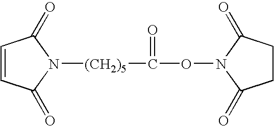
[0124] After cooling the substrate, it was immersed into a 0.3% solution (ethanol:dimethylsulfoxide=1:1) of N-(6-maleimidecaproxy)succinimide (EMCS: compound II)
[0125] for ...
example 3
[Formation of Black Matrix]
[0133] Black resist (CK-A143B Resist: tradename, available from FUJIFILM Arch Co., Ltd.) containing carbon black was applied onto a glass substrate (1737: tradename, available from Corning) and subjected to a predetermined exposure session using a UV aligner and a developing operation using an inorganic aqueous alkali solution. Then, the substrate was heated in a clean oven at 220° C. for 60 minutes and subjected to a post bake treatment to prepare a black matrix pattern (division wall) having a film thickness of 2 μm and rectangular openings of 100 μm×200 μm. The length a of the division wall was made equal to 20 μm.
[Evaluation of Surface Coarseness]
[0134] The surface coarseness of the glass substrate used for forming the black matrix was observed at arbitrarily selected areas by using NanoScope IIIa AFM Dimension 3000 Stage System (tradename, available from Digital Instrument) before forming the black matrix. As a result, the substrate showed an avera...
PUM
| Property | Measurement | Unit |
|---|---|---|
| temperature | aaaaa | aaaaa |
| contact angle | aaaaa | aaaaa |
| contact angle | aaaaa | aaaaa |
Abstract
Description
Claims
Application Information