Conductive sintered compact for fixing electrodes in electronic device envelope

Inactive Publication Date: 2005-07-28
FUTABA CORPORATION
View PDF3 Cites 2 Cited by
  • Summary
  • Abstract
  • Description
  • Claims
  • Application Information

AI Technical Summary

Benefits of technology

[0034] According to the present invention, a relatively thick conductive thin film, or a conductive sintered compact, having a thickness of 300 μm or more can be easily formed to anchor electrodes in an electronic device envelope, for example, in a fluoresc

Problems solved by technology

Thus, the conductive paste itself is dried and loses its viscosity.
According to one theory, differences i

Method used


Image

  • Conductive sintered compact for fixing electrodes in electronic device envelope
  • Conductive sintered compact for fixing electrodes in electronic device envelope
  • Conductive sintered compact for fixing electrodes in electronic device envelope

Examples


Embodiment Construction

[0061] A conductive sintered material for fixing electrodes in electronic device envelopes, according to an embodiment of the present invention, will be described below in detail. Moreover, the case where a conductive material formed of a conductive compound is embodied to intermediately-bonded electrodes in a fluorescent display tube will also be described below in more detail.

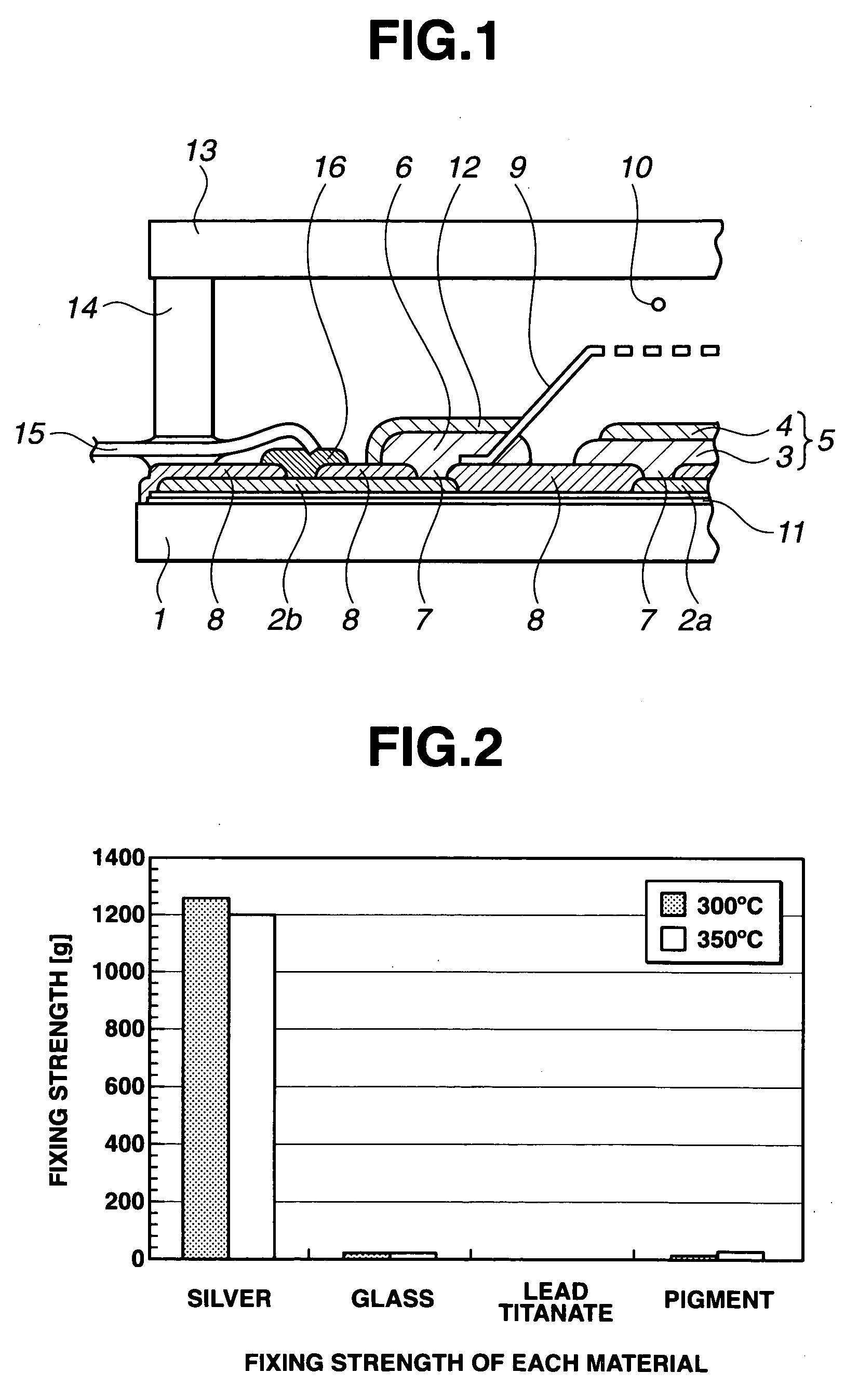
[0062] The main configuration of a fluorescent display tube applied to the present embodiment is shown in FIG. 1. The previous explanation is applicable to this detailed description. Further detailed explanation will be later added to the previous description.

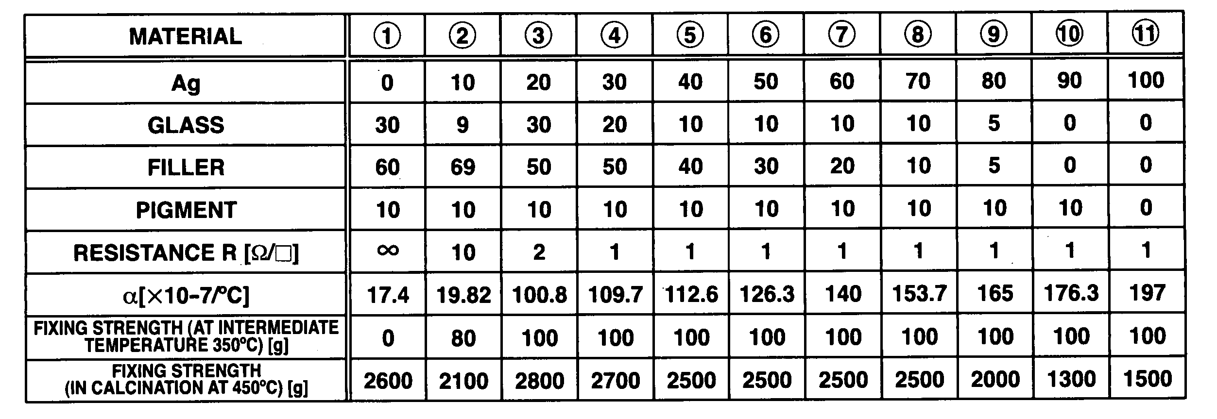
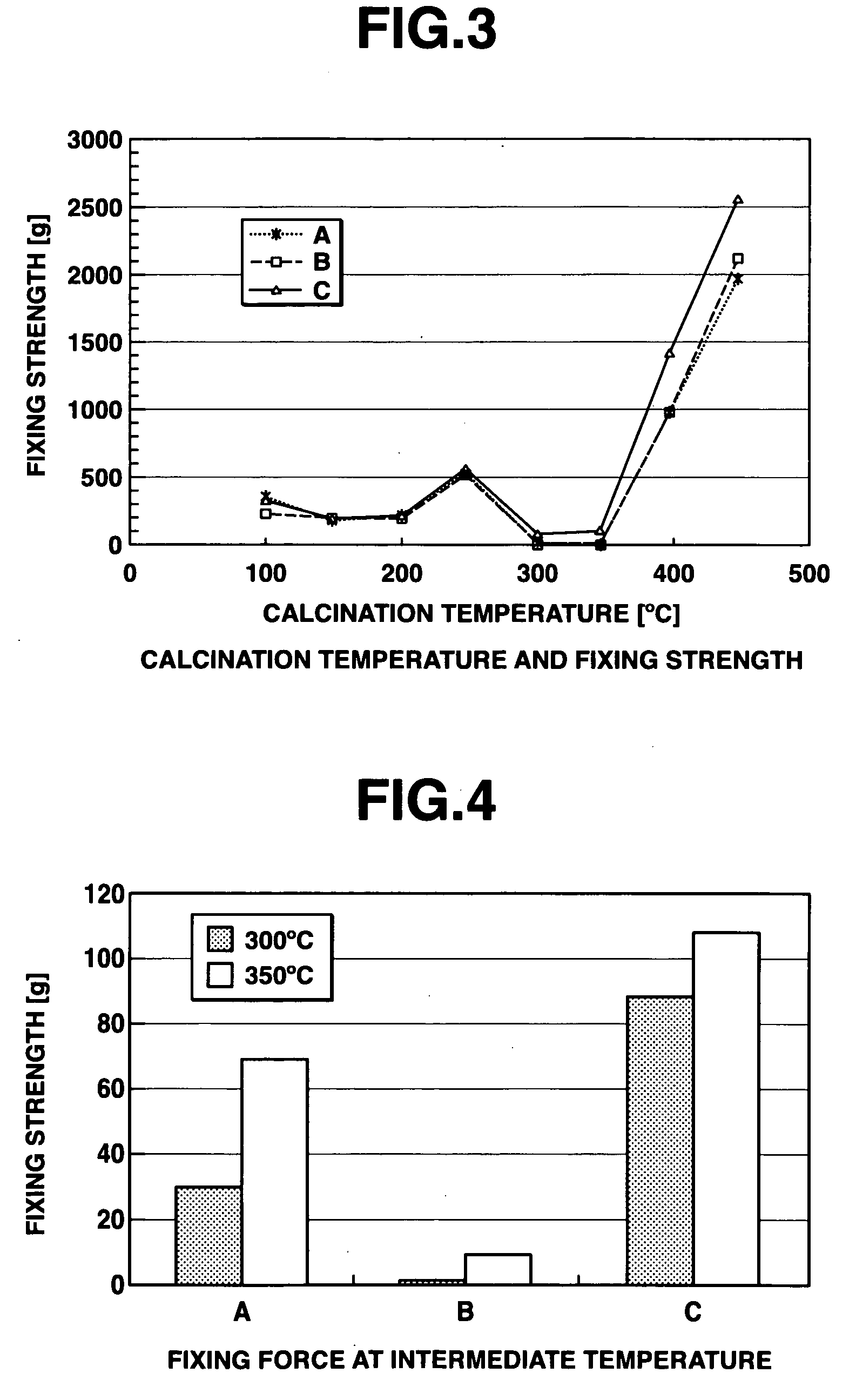
[0063]FIG. 2 shows measured fixing strengths of Ag particles constituting a conductive compound, a PbO—B2O3 series low-melting-point glass, and lead titanate, and a metal oxide series pigment, sintered at 300° C. and 350° C., respectively.

[0064] Referring to FIG. 2, Ag particles, a PbO—B2O3 series low-melting point glass, lead titanate, and metal oxid...


PUM

PropertyMeasurementUnit
Electrical resistanceaaaaaaaaaa
Electrical conductoraaaaaaaaaa
Melting pointaaaaaaaaaa

Abstract

A conductive sintered compact for fixing electrodes inside an electronic device envelope is provided. The sintered compact is made of a conductive composition calcined. The conductive composition includes at least 10 vol % to 60 vol % of Ag particles, a low melting-point glass containing 10 vol % to 80 vol % of B2O3, 0 vol % to 70 vol % of ceramic particles, and a metal oxide series pigment. The total amount of the ceramic particles and the metal oxide series pigment is at least 10 vol % or more.

Description

CROSS REFERENCES TO RELATED APPLICATIONS [0001] Not Applicable. STATEMENT REGARDING FEDERALLY SPONSORED RESEARCH [0002] Not Applicable. BACKGROUND OF THE INVENTION [0003] The present invention relates to a conductive sintered compact for fixing electrodes in an electronic device envelope. More particularly, the present invention relates to a conductive fixing member for arranging electrodes mounted on predetermined areas in an electronic device envelope. For example, the present invention relates to a conductive sintered compact used to fix grid electrodes on the surface of an insulating substrate disposed inside a fluorescent display tube envelope. [0004] Conventionally, conductive fixing members acting as internal wiring layers are used inside an envelope constituting a fluorescent display tube or the like to arrange various electrodes over the insulating substrate therein. [0005] Usually, in order to prepare a conductive paste, Ag particles, acting as a conductive material, and a...

Claims


Application Information

Patent Timeline
IPC IPC(8): H01B1/08C03C14/00H01B1/06H01B1/16H01J9/18H01J29/02H01J31/15H01L23/48
CPCB22F3/225C03C14/004H01J2329/00C03C2214/08H01J9/18C03C2214/04B05C17/00516B05C17/0052
Inventor MISONOU, TOSHIYUKIKATO, MASAHIRO
Owner FUTABA CORPORATION
Why Eureka
Try Eureka