Organic electroluminescence display apparatus

a display apparatus and electroluminescence technology, applied in the direction of discharge tube luminescnet screens, discharge tube/lamp details, electric discharge lamps, etc., can solve the problems of complexity, damage to mask pattern m, and decrease in yield in manufacturing flat display apparatuses, etc., to achieve the effect of improving yield

Inactive Publication Date: 2005-07-28
UDC IRELAND +1
View PDF15 Cites 28 Cited by
  • Summary
  • Abstract
  • Description
  • Claims
  • Application Information

AI Technical Summary

Benefits of technology

[0028] With the present invention, by forming a recess portion in an insulation film having an organic EL element covering a thin film transistor, and thus by forming the recess portion in an organic EL layer, an evaporation mask used in forming a lower electrode or an organic EL layer can be prevented from physically contacting the formed lower electrode or organic EL layer. Accordingly, an improved yield can be attained in manufacturing an organic EL flat display apparatus of an active matrix type.

Problems solved by technology

Accordingly, the extremely thin organic EL layers are susceptible to damage, thereby leading to decrease of yield in manufacturing the flat display apparatus.
Furthermore, the physical contact with the organic EL layers may also damage the mask pattern M. Accordingly, in such a case where the mask pattern M is damaged, defects created by such damage are transferred to all pixels formed later on.
Furthermore, in the step shown in FIG. 2A, the mask pattern M also contacts the lower electrode 172 and 173, thereby leading to damage thereof.
The formation of the partitions 23, however, has problems of being complicated, requiring extra steps such as deposition of an insulation layer and patterning, etc., and increasing manufacturing cost of the flat display apparatus.

Method used


Image

  • Organic electroluminescence display apparatus
  • Organic electroluminescence display apparatus
  • Organic electroluminescence display apparatus

Examples


first embodiment

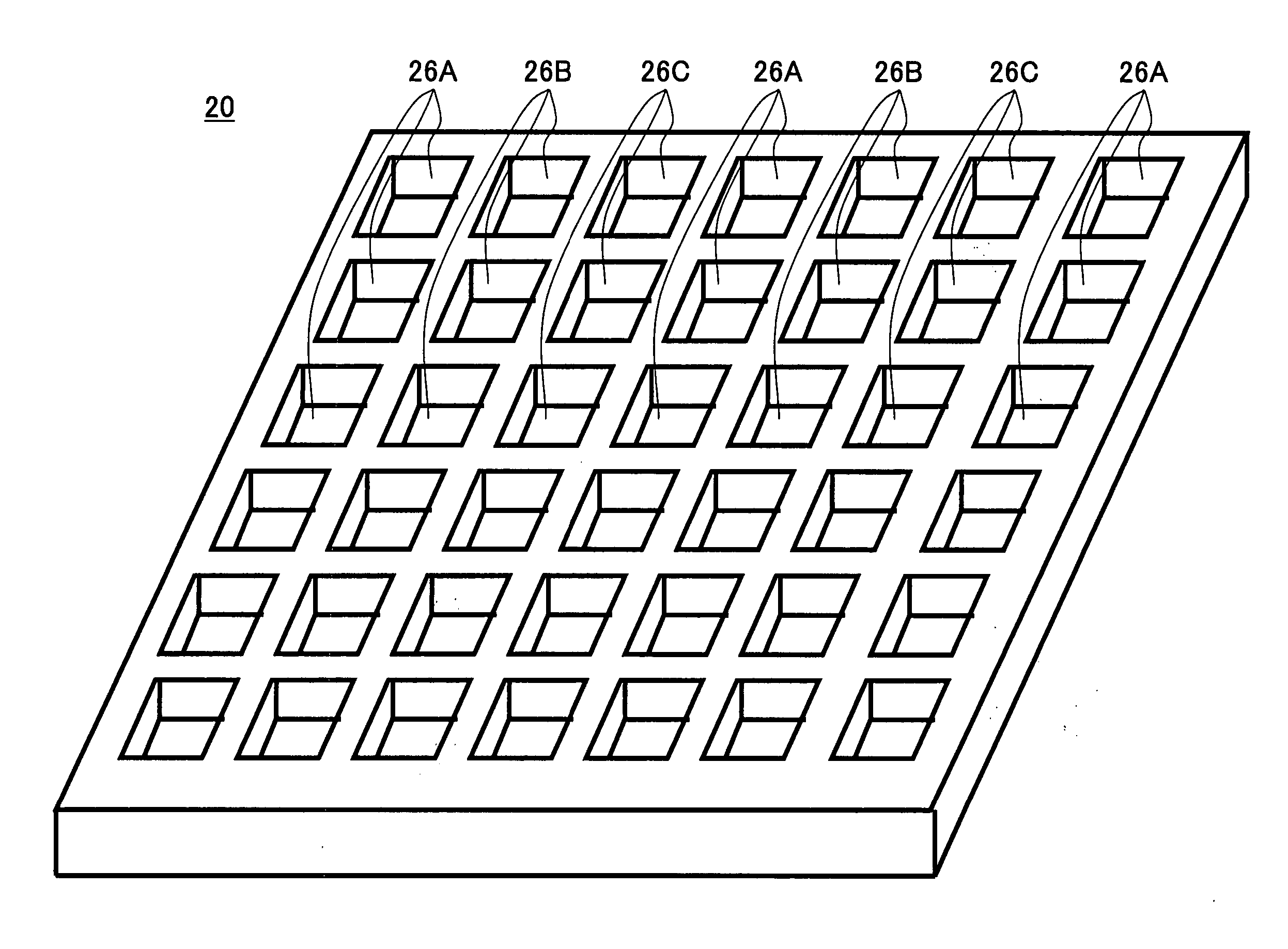
[0038]FIGS. 4A-4G show a process of manufacturing an organic EL flat display apparatus 20 according to a first embodiment of the present invention. In the drawings, however, reference numbers of the above-described components are denoted with the same references numbers and description thereof is omitted.

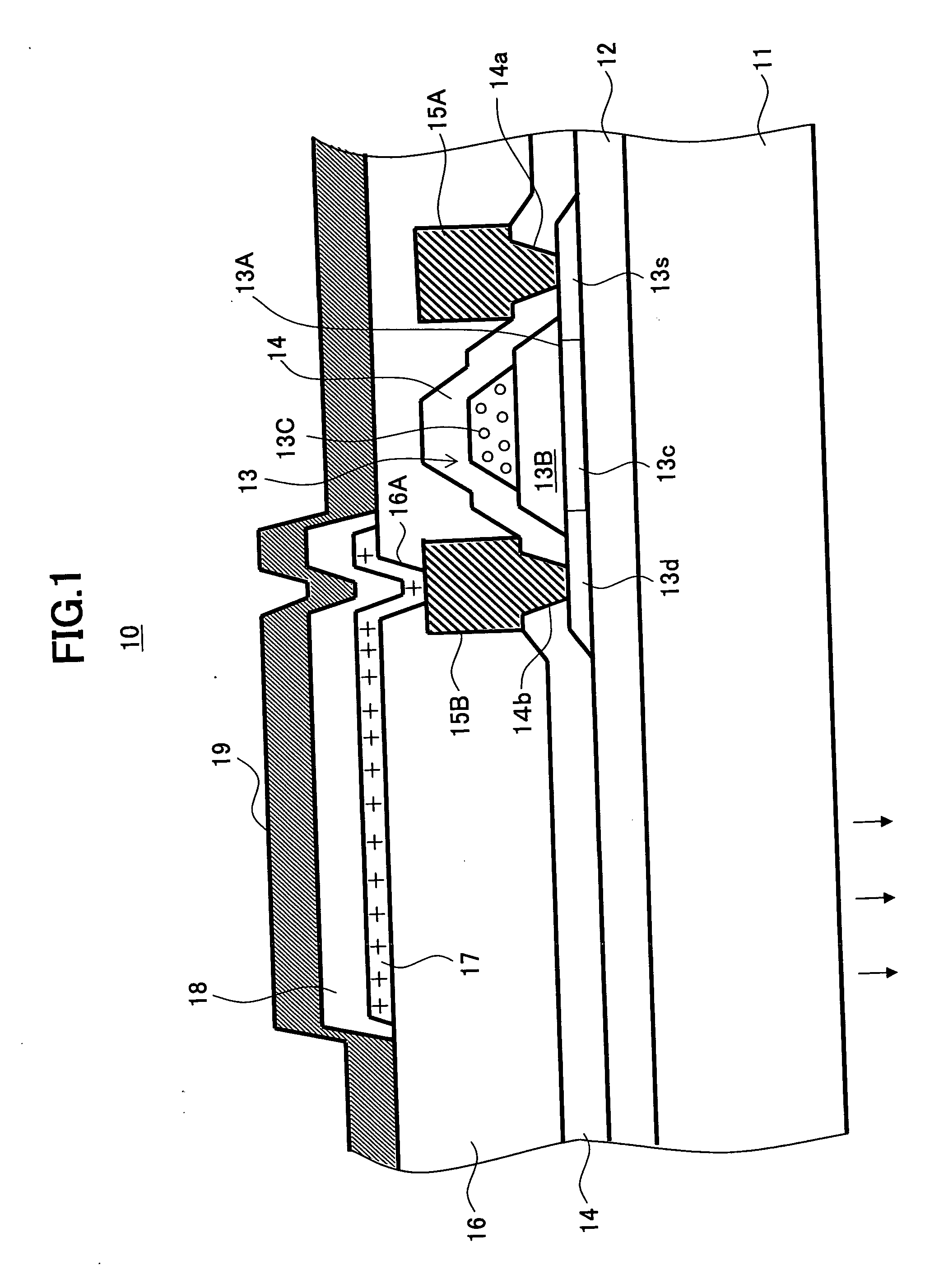
[0039] With reference to FIG. 4A, a TFT 13 is formed on a glass substrate 11 via a buffer layer 12 formed of, for example, SiO2. The TFT 13 is covered by a CVD insulation film 14 formed by a low temperature process such plasma CVD.

[0040] In the step shown in FIG. 4A, a photosensitive planarized film 26, including, for example, acrylic resin or resist film, is coated on the CVD insulation film 14 to a thickness of 2-3 μm, or example, by employing a typical coating method. The planarized film 26 formed in such manner has a characteristic of having a planar surface.

[0041] Furthermore, in the step shown in FIG. 4A, the planarized film 26 is exposed to ultraviolet light with use of an...

second embodiment

[0057]FIG. 7 is an organic EL flat display apparatus 40 according to a second embodiment of the present invention. In this embodiment, a gate electrode 41A, being formed of amorphous silicon or polysilicon, is disposed on a buffer layer 12 covering the glass substrate 11, and an insulation film 41B, serving as a gate insulation film, is formed on the buffer layer 12 in a manner covering the polysilicon gate electrode 41A.

[0058] Furthermore, a semiconductor layer 41C, being formed of amorphous silicon or polysilicon, is disposed on the insulation film 41B, and an insulation film pattern 41D is disposed on the semiconductor layer 41C at a position corresponding to the gate electrode 41A. By adding an impurity element by ion injection with the insulation pattern 41D as a mask, a source area 41s and a drain area 41d are formed in the semiconductor layer 41C in a state separated by a channel area 41c situated therebetween.

[0059] Furthermore, the semiconductor layer 41C is covered by th...

third embodiment

[0064]FIG. 8 shows a process of manufacturing an organic EL flat display apparatus 60 according to a third embodiment of the present invention. In the drawing, however, reference numbers of the above-described components are denoted with the same references numbers and description thereof is omitted.

[0065] The process shown in FIG. 8 corresponds to the processes shown in FIGS. 4A and 4B. In this embodiment, instead of the photosensitive film 26, an insulation film 16 having no photosensitivity, such as a normal plasma CVD-SiO2 film, is used as the planarized insulation film.

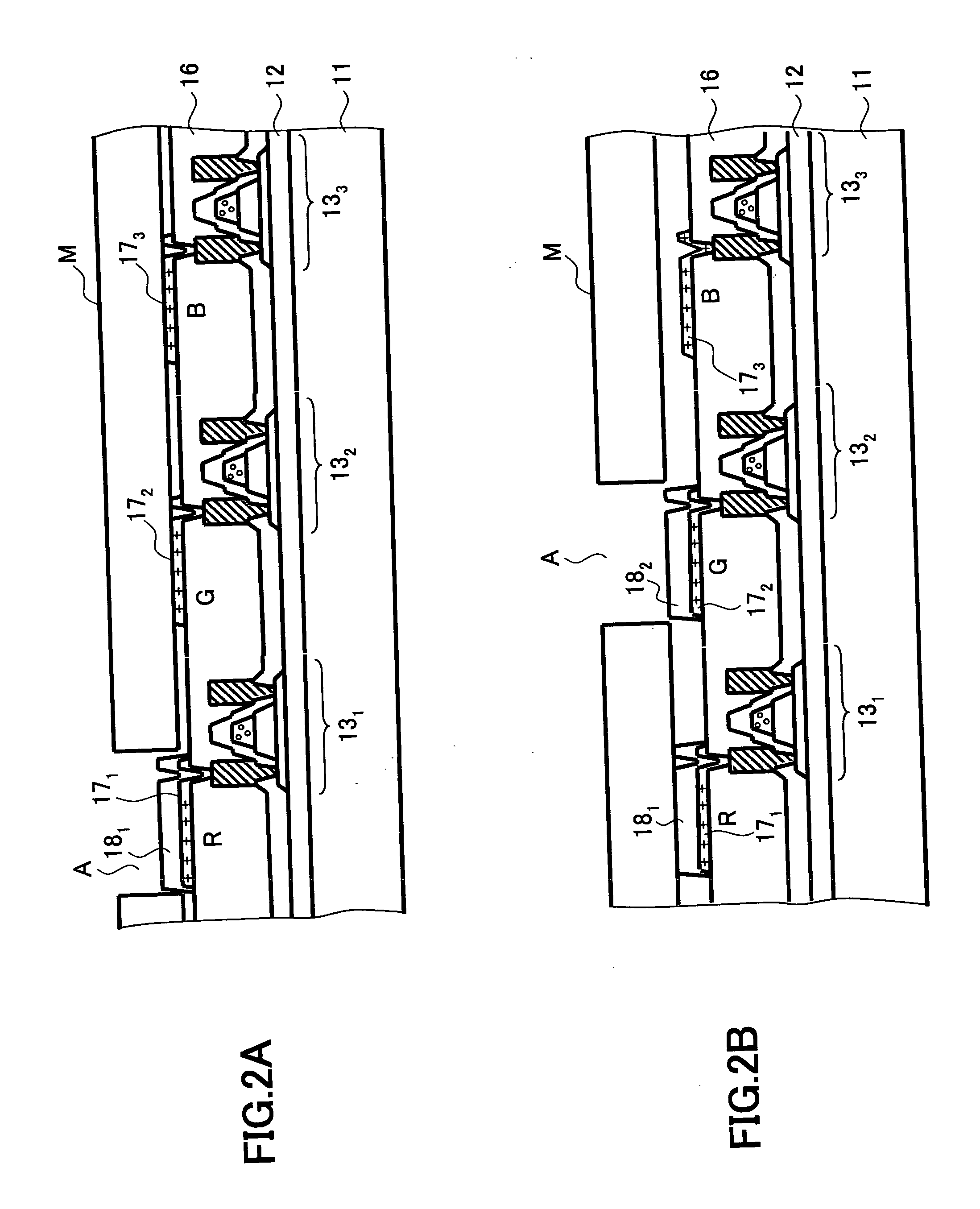
[0066] Accordingly, in the process shown in FIG. 8, a resist pattern R is formed on the insulation film 16. By wet-etching the insulation film 16 with the resist pattern R as a mask, a recess portion 16A is formed in the insulation film 16.

[0067] Processes following this process are the same as those of the foregoing embodiment. This embodiment also enables an organic EL flat display apparatus of an active mat...


PUM


Abstract

An organic EL display apparatus is disclosed that includes a substrate, a thin film transistor formed on the substrate, an insulation film formed on the substrate in a manner covering the thin film transistor, and an organic EL element formed on the insulation film. The insulation film is formed with a recess portion. The organic EL element is formed in a manner contacting the thin film transistor via the recess portion formed in the insulation film.

Description

CROSS-REFERENCE TO RELATED APPLICATIONS [0001] This application is a U.S. continuation application filed under 35 USC 111(a) claiming benefit under 35 USC 120 and 365(c) of PCT application JP 2003 / 04776, filed Apr. 15, 2003. The foregoing application is hereby incorporated herein by reference.BACKGROUND OF THE INVENTION [0002] 1. Field of the Invention [0003] The present invention relates to an organic electroluminescence display apparatus, and more particularly to a flat display apparatus using an organic electroluminescence element. [0004] An organic EL (electroluminescence) element is an organic light emitting element having an organic EL light emitting layer sandwiched between an electron transport layer and a hole transport layer, and is considered to be a promising display serving as a light emitting type display element that is small / lightweight / low power consuming and also provides a wide viewing angle. [0005] In a case of forming a high definition flat light emitting appara...

Claims


Application Information

Patent Timeline
Patent Type & Authority Applications(United States)
IPC IPC(8): H01J1/62H01J63/04H01L27/32H01L51/52H01L51/56H05B33/12H05B33/14H05B33/22
CPCH01L27/3211H01L27/3246H01L51/56H01L27/3258H01L27/3248H10K59/35H10K59/123H10K59/124H10K59/122H10K71/00
Inventor YAEGASHI, HIROYUKI
Owner UDC IRELAND
Why Eureka
Try Eureka