Film substrate, fabrication method thereof, and image display substrate

Inactive Publication Date: 2005-08-04
PANASONIC CORP
View PDF3 Cites 11 Cited by
  • Summary
  • Abstract
  • Description
  • Claims
  • Application Information

AI Technical Summary

Benefits of technology

[0010] The present invention accordingly solves these problems and it is an object thereof to provide a film substrate that makes it possible to reduce the pitch of the conductive wiring portion, secure i

Problems solved by technology

As a result, short circuit failure between electrodes of the substrate of the liquid crystal display

Method used


Image

  • Film substrate, fabrication method thereof, and image display substrate
  • Film substrate, fabrication method thereof, and image display substrate
  • Film substrate, fabrication method thereof, and image display substrate

Examples


Example

[0023] Embodiments of the present invention will be described hereinafter with reference to the drawings.

Film Substrate

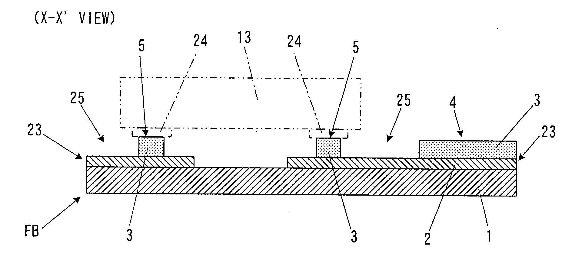
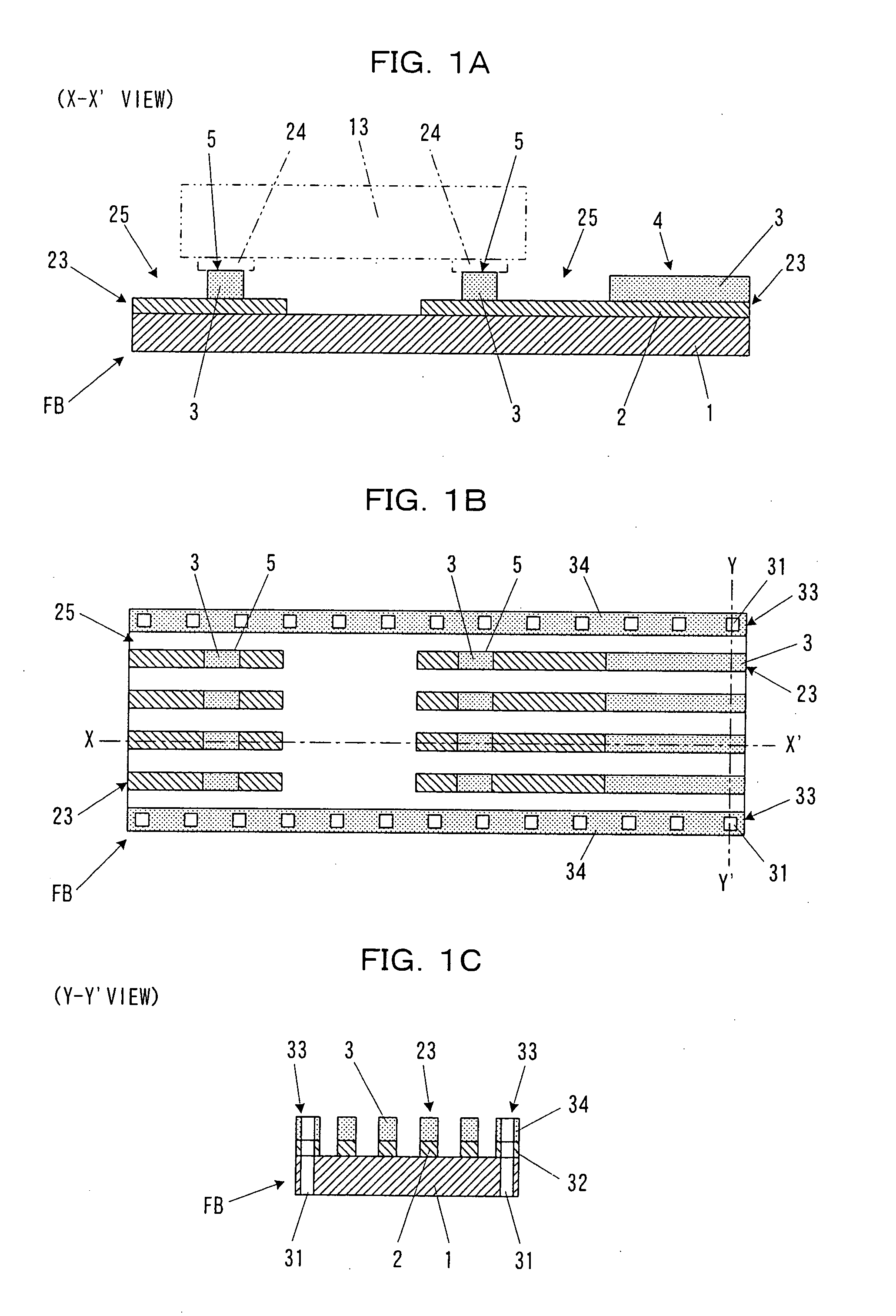
[0024]FIG. 1A to 1C each shows a part of the film substrate of an embodiment of the present invention.

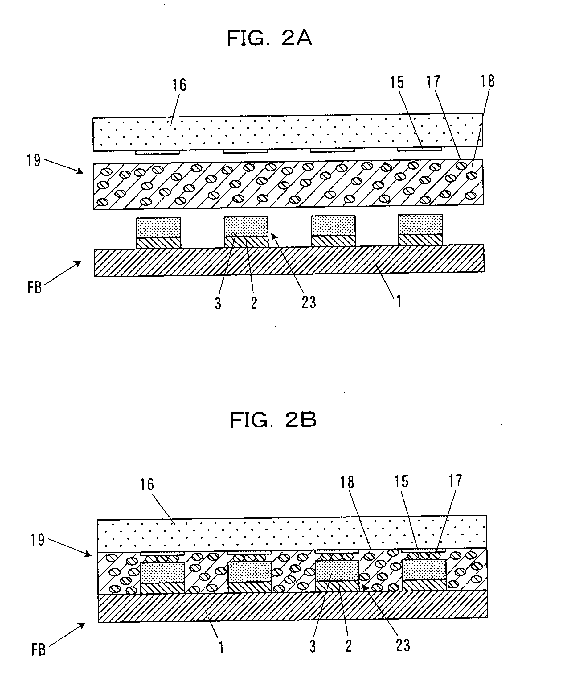
[0025] In FIGS. 1A to 1C, FB is a film substrate on which a semiconductor element 13 is mounted. The film substrate FB consists of a flexible and insulating film base material 1 and conductor wiring 23 that is formed on the film base material 1 and to which the semiconductor element 13 is connected.

[0026] The conductor wiring 23 comprises, for example, external connection portions 4 on the film substrate that are joined to electrodes (or terminals) 15 of an image-display flat panel (liquid crystal display panel; an example of another panel) 16 shown in FIG. 3 and the electrodes (or terminals) 21 of a print substrate (an example of another substrate) 20 of the image-display flat panel 16; and semiconductor connection portions (mount portions) 5 to which the semic...


PUM


Abstract

In a film substrate (FB) including a film base material (1) and conductor wiring (23) that is formed on the film base material (1), the conductor wiring (23) is arranged such that the conductor wiring thickness of an external connection portion on the film substrate to which another panel or substrate is connected is thicker than the conductor wiring thickness of conductor wiring portions (bent portions) (25) at other positions.

Description

BACKGROUND OF THE INVENTION [0001] 1. Field of the Invention [0002] The present invention relates to a film substrate that is mounted in an image display flat panel or the like and, more particularly, to a conductor-wiring structure for the film substrate and the fabrication method thereof. [0003] 2. Description of the Related Art [0004] One form of semiconductor package that is mounted in an image display flat panel or the like is a tape carrier package, which is mainly used as a driver for driving purposes. Among such tape carrier packages, a tape carrier package in which holes in the film base material are not formed in semiconductor element mount portions of the film base material in particular is known as COF (Chip On Film; a mounting structure that uses a thin film for the substrate and in which the chip and circuit on the film substrate are electrically connected by means of bumps). [0005] A commonly known film substrate with the COF structure is disclosed in Japanese Patent ...

Claims


Application Information

Patent Timeline
IPC IPC(8): H01L21/60G02F1/13G02F1/1345H01L23/34H01L23/498H05K1/00H05K1/02H05K1/11H05K3/00H05K3/10H05K3/24H05K3/36
CPCG02F1/13452H01L23/4985H01L2924/00013H01L2224/16225H01L2224/293H01L2224/2929H01L2924/014H01L2924/01033H01L2924/01019H01L2924/01006H01L24/29H05K2203/0574H05K2201/2009H01L24/83H01L2224/83101H01L2224/838H01L2924/01005H01L2924/01029H01L2924/01078H01L2924/01079H01L2924/0781H01L2924/19043H05K1/0263H05K1/0265H05K1/0281H05K1/111H05K1/117H05K1/189H05K3/0097H05K3/108H05K3/243H05K3/361H05K2201/09063H05K2201/09736H05K2201/09781H05K2201/10674H01L2924/00014H01L2224/29099H01L2224/29199H01L2224/29299H01L2224/05568H01L2224/05573H01L2224/0615H05K2201/056H05K2201/10128H05K2201/10681H01L2224/05599G02F1/1345
Inventor IMAMURA, HIROYUKI
Owner PANASONIC CORP
Why Eureka
Try Eureka