Radiation detector assembly, lithographic apparatus, method of determining an amount of radiation, an intensity of the amount of radiation, or an amount of contamination of an optical element, device manufacturing method, and device manufactured thereby

a technology of lithographic apparatus and detector assembly, which is applied in the direction of photometry, instruments, photographic processes, etc., can solve the problems of radiation absorbers, and achieve the effect of convenient and reliable, at more optical components

Inactive Publication Date: 2005-08-11
ASML NETHERLANDS BV
View PDF7 Cites 24 Cited by
  • Summary
  • Abstract
  • Description
  • Claims
  • Application Information

AI Technical Summary

Benefits of technology

[0009] It is an aspect of the present invention to provide an assembly for determining EUV radiation flux in a lithogra

Problems solved by technology

In particular for EUV radiation, a problem is that the substrate, th

Method used


Image

  • Radiation detector assembly, lithographic apparatus, method of determining an amount of radiation, an intensity of the amount of radiation, or an amount of contamination of an optical element, device manufacturing method, and device manufactured thereby
  • Radiation detector assembly, lithographic apparatus, method of determining an amount of radiation, an intensity of the amount of radiation, or an amount of contamination of an optical element, device manufacturing method, and device manufactured thereby
  • Radiation detector assembly, lithographic apparatus, method of determining an amount of radiation, an intensity of the amount of radiation, or an amount of contamination of an optical element, device manufacturing method, and device manufactured thereby

Examples


Embodiment Construction

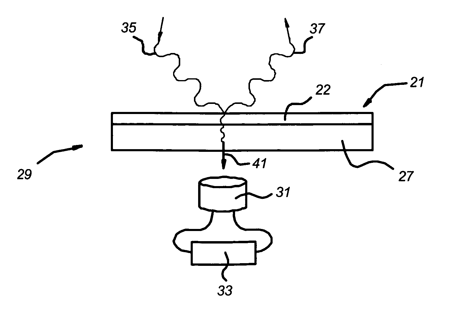
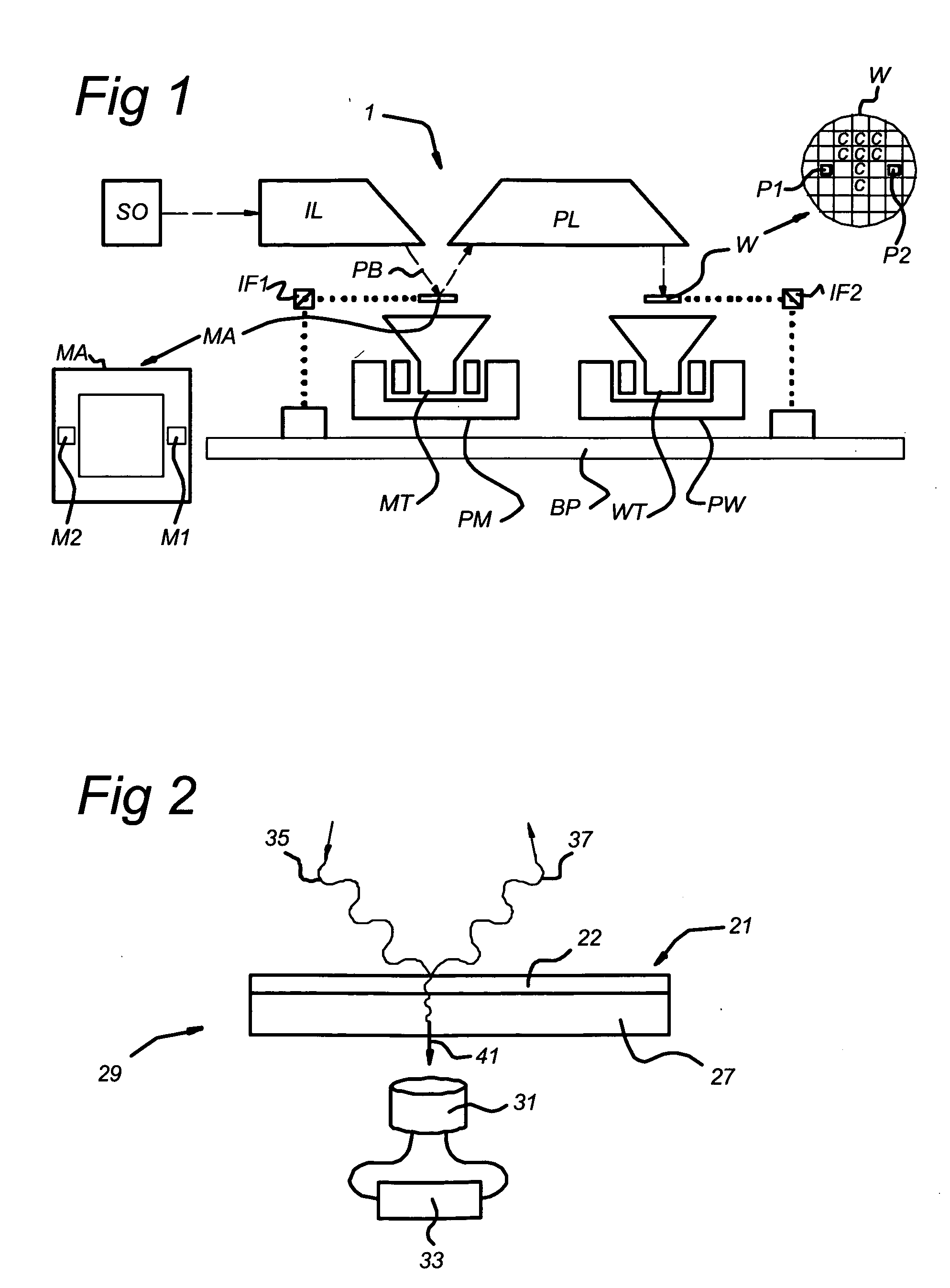
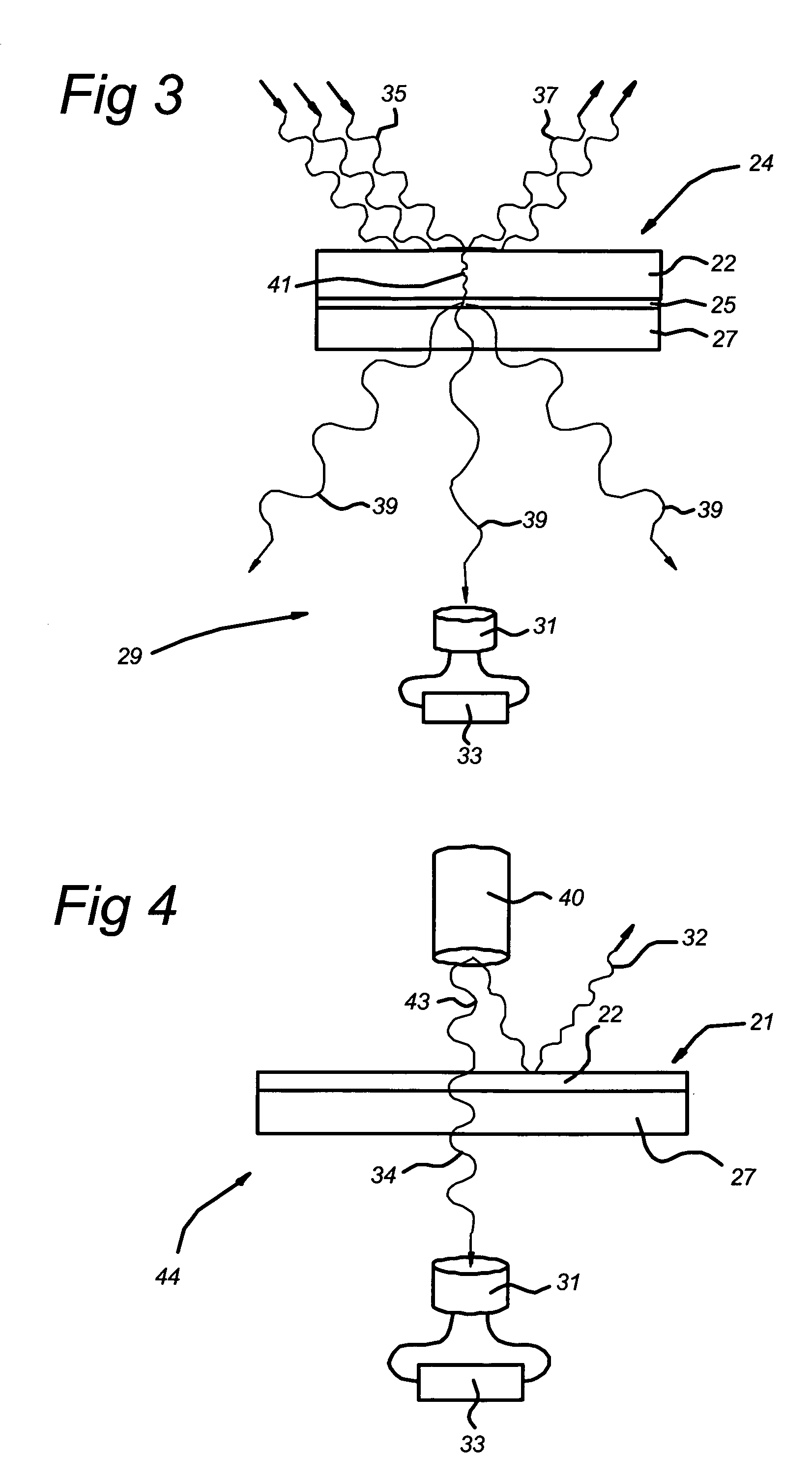
[0035]FIG. 1 schematically depicts a lithographic apparatus 1 according to an embodiment of the invention. The apparatus includes a base plate BP. An illumination system (illuminator) IL is configured to provide a beam of radiation PB of radiation (e.g. UV or EUV radiation). A support (e.g. a mask table) MT is configured to support a patterning device (e.g. a mask) MA and is connected to a first positioning device PM that accurately positions the patterning device with respect to a projection system PL. A substrate table (e.g. a wafer table) WT is configured to hold a substrate (e.g. a resist-coated wafer) W and is connected to a second positioning device PW that accurately positions the substrate with respect to the projection system PL. The projection system (e.g. a reflective projection lens) PL is configured to image a pattern imparted to the beam of radiation PB by patterning device MA onto a target portion C (e.g. including one or more dies) of the substrate W.

[0036] As here ...


PUM


Abstract

A radiation detector assembly includes an optical element including a substrate and a partially reflective optical layer. The optical element is configured to receive an amount of radiation when the assembly is in use and reflect a first portion of the amount of radiation and transmit a second portion of the amount of radiation through the optical layer and the substrate. A radiation detector is configured to receive the second portion of the amount of radiation and provide a measurement signal. A measurement system is configured to receive the measurement signal from the radiation detector and derive from the measurement signal the amount of radiation, an intensity of the amount of radiation, or an amount of contamination of the optical layer.

Description

CROSS REFERENCE TO RELATED APPLICATIONS [0001] This application claims priority to European Patent Application 03078516.6, filed Nov. 7, 2003, the contents of which are incorporated herein by reference. BACKGROUND OF THE INVENTION [0002] 1. Field of the Invention [0003] The present invention relates to a radiation detector assembly, a lithographic apparatus, a method of determining an amount of radiation, an intensity of the amount of radiation, or an amount of contamination of an optical element receiving the amount of radiation, a device manufacturing method, and a device manufacture thereby. [0004] 2. Description of the Related Art [0005] A lithographic apparatus is a machine that applies a desired pattern onto a target portion of a substrate. Lithographic apparatus can be used, for example, in the manufacture of integrated circuits (ICs). In that circumstance, a patterning device, such as a mask, may be used to generate a circuit pattern corresponding to an individual layer of t...

Claims


Application Information

Patent Timeline
IPC IPC(8): G01T1/20G01J1/42G03F7/20H01L21/027
CPCG03F7/70558G03F7/70916G03F7/7085G01J1/42G03F7/20
Inventor BAKKER, LEVINUS PIETER
Owner ASML NETHERLANDS BV
Why Eureka
Try Eureka