Micro pin grid array with pin motion isolation

a micro-pin grid array and pin technology, applied in the field of micro-electronic package making and testing, can solve the problem of rubbing the tip of the post across, and achieve the effect of facilitating the flexing of the substrate and facilitating the movement of the terminals

Inactive Publication Date: 2005-08-11
TESSERA INC
View PDF66 Cites 151 Cited by
  • Summary
  • Abstract
  • Description
  • Claims
  • Application Information

AI Technical Summary

Benefits of technology

[0016] In certain preferred embodiments of the present invention a microelectronic package includes a microelectronic element, such as a semiconductor chip, having faces and contacts, and a flexible substrate overlying and spaced from a first face of the microelectronic element. The flexible substrate may include a dielectric sheet or a polymeric film. The package also preferably includes a plurality of conductive terminals exposed at a surface of the flexible substrate, the conductive terminals being electrically interconnected with the microelectronic element. In this aspect of the invention, the flexible substrate most desirably includes a gap extending at least partially around at least one of the conductive terminals and defining a region holding one or more terminals which region can be displaced at least partially independently of the remainder of the substrate. In preferred embodiments according to this aspect of the present invention, the gap facilitates flexing of the substrate, and thus facilitates movement of the terminals. This action is useful during engagement of the terminals with a test fixture.

Problems solved by technology

As further discussed below, this can cause the tips of the posts to wipe across the surfaces of terminals on a test circuit board.

Method used


Image

  • Micro pin grid array with pin motion isolation
  • Micro pin grid array with pin motion isolation
  • Micro pin grid array with pin motion isolation

Examples


Embodiment Construction

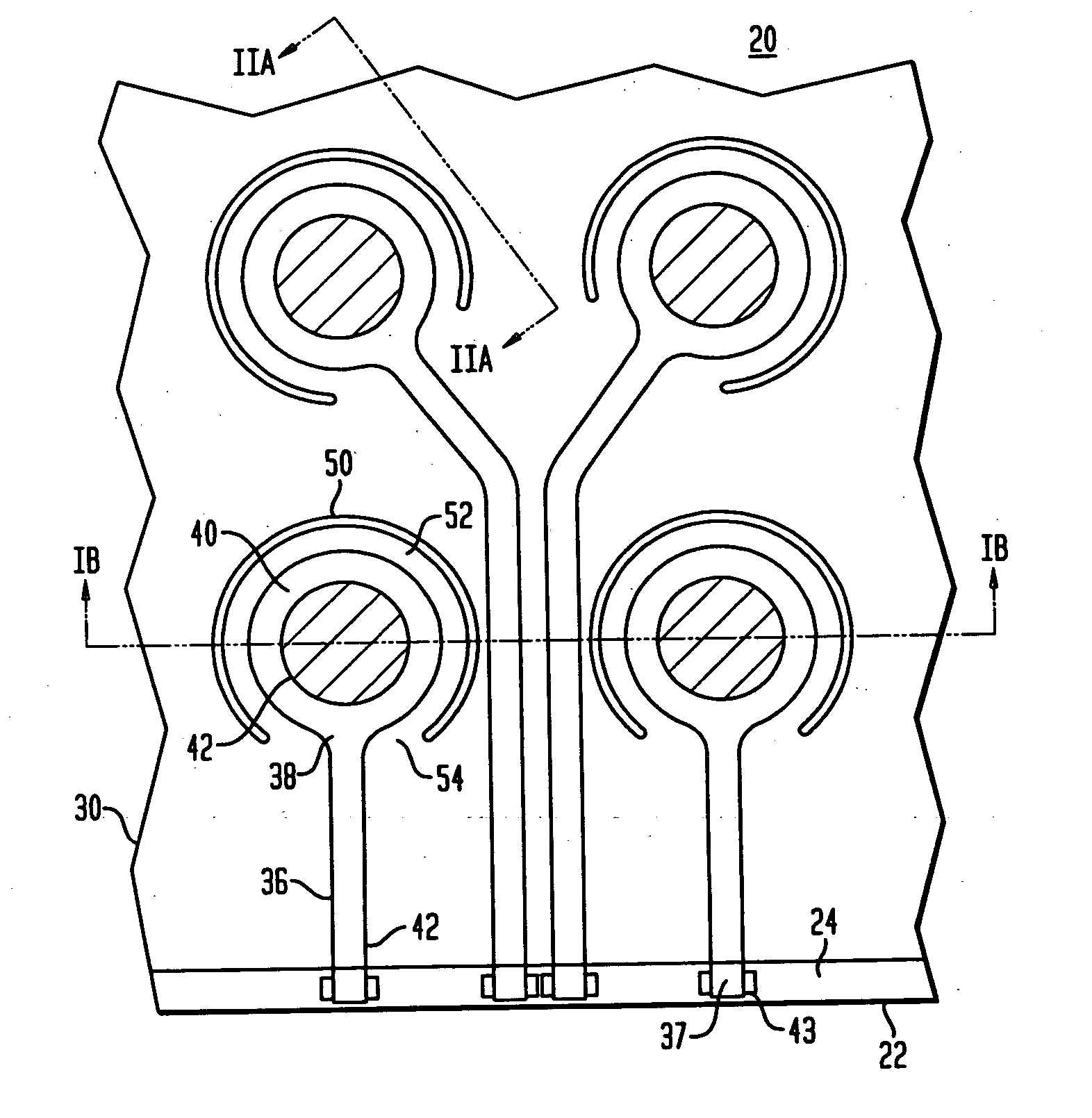
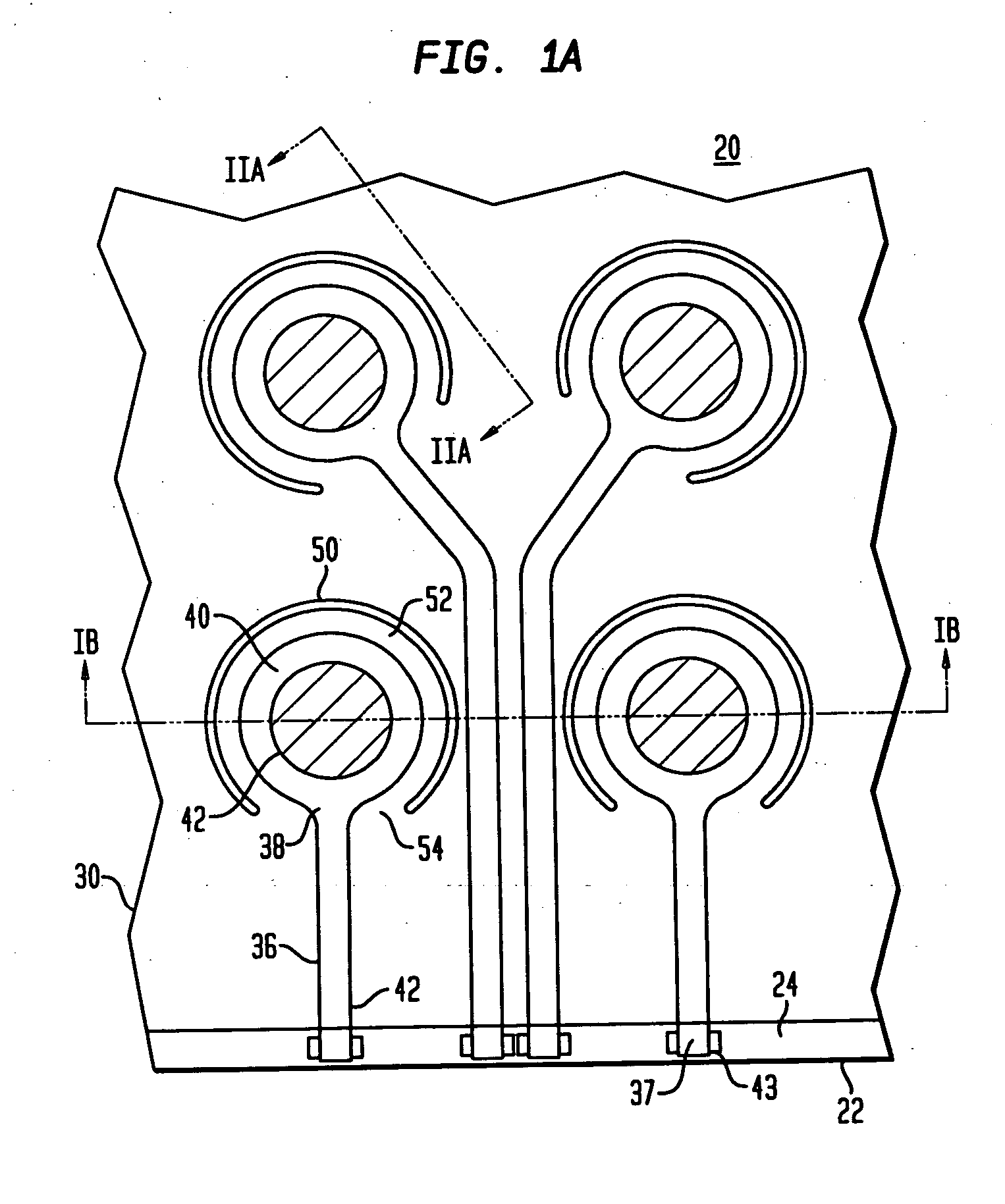
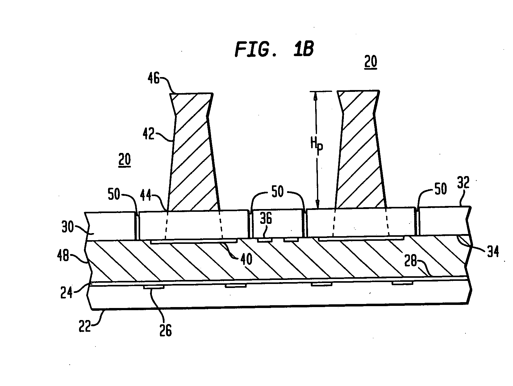
[0049] Referring to FIGS. 1A and 1B, a microelectronic package 20 in accordance with one embodiment of the present invention includes a microelectronic element 22 such as a semiconductor chip having a front or contact-bearing face 24 and electrical contacts 26 exposed at the face 24. A passivation layer 28 may be formed over the contact-bearing face 24 with openings at contacts 26.

[0050] The microelectronic package 20 preferably includes a flexible dielectric substrate 30, such as a polyimide or other polymeric sheet, including a top surface 32 and a bottom surface 34 remote therefrom. Although the thickness of the dielectric substrate 30 may vary depending upon the application, the dielectric substrate most typically is about 15-100 μm thick. The flexible sheet 30 has conductive traces 36 thereon. In the particular embodiment illustrated in FIGS. 1A and 1B, the conductive traces are disposed on the bottom surface 34 of the flexible sheet 30. However, in other embodiments, the cond...


PUM


Abstract

A microelectronic package includes a microelectronic element having faces and contacts, a flexible substrate overlying and spaced from a first face of the microelectronic element, and a plurality of conductive terminals exposed at a surface of the flexible substrate. The conductive terminals are electrically interconnected with the microelectronic element and the flexible substrate includes a gap extending at least partially around at least one of the conductive terminals. In certain embodiments, the package includes a support layer, such as a compliant layer, disposed between the first face of the microelectronic element and the flexible substrate. In other embodiments, the support layer includes at least one opening that is at least partially aligned with one of the conductive terminals.

Description

CROSS REFERENCE TO RELATED APPLICATIONS [0001] The present application claims the benefit of the filing date of U.S. Provisional Application No. 60 / 533,437 filed Dec. 30, 2003, the disclosure of which is hereby incorporated herein by reference.FIELD OF THE INVENTION [0002] The present invention generally relates to microelectronic packages and more specifically to methods of making and testing microelectronic packages. BACKGROUND OF THE INVENTION [0003] Microelectronic devices such as semiconductor chips typically require many input and output connections to other electronic components. The input and output contacts of a semiconductor chip or other comparable device are generally disposed in grid-like patterns that substantially cover a surface of the device (commonly referred to as an “area array”) or in elongated rows which may extend parallel to and adjacent each edge of the device's front surface, or in the center of the front surface. Typically, devices such as chips must be ph...

Claims


Application Information

Patent Timeline
Patent Type & Authority Applications(United States)
IPC IPC(8): H01L21/44H01L23/48H01L23/498H05K1/11H05K3/32H05K3/34
CPCH01L23/49811H01L23/49838H01L23/4985H05K1/118H05K3/326H05K3/3436H05K2201/0133H01L2924/0002H05K2201/0367H05K2201/09063H05K2201/09081H05K2201/10674H01L2924/00
Inventor DAMBERG, PHILIPHABA, BELGACEMTUCKERMAN, DAVID B.KANG, TECK-GYU
Owner TESSERA INC
Why Eureka
Try Eureka