Memory device

a memory device and memory technology, applied in the field of memory devices, can solve the problems of difficult acceleration of operation speed, large time requirement, and time-consuming, and achieve the effect of simple configuration

Active Publication Date: 2005-08-11
SONY CORP
View PDF9 Cites 27 Cited by
  • Summary
  • Abstract
  • Description
  • Claims
  • Application Information

AI Technical Summary

Benefits of technology

[0037] Therefore, according to the present invention, it is possible to perform the multi-value recording at a high speed and the

Problems solved by technology

However, since a writing operation in the flash memory is performed by injecting in stages an electric charge into a terminal called a floating gate, considerably large amount of time is required compared with a case of performing 1-bit recording (single-value recording) when the flash memory is used to perform the multi-value recording.
Furth

Method used


Image

  • Memory device
  • Memory device
  • Memory device

Examples


Embodiment Construction

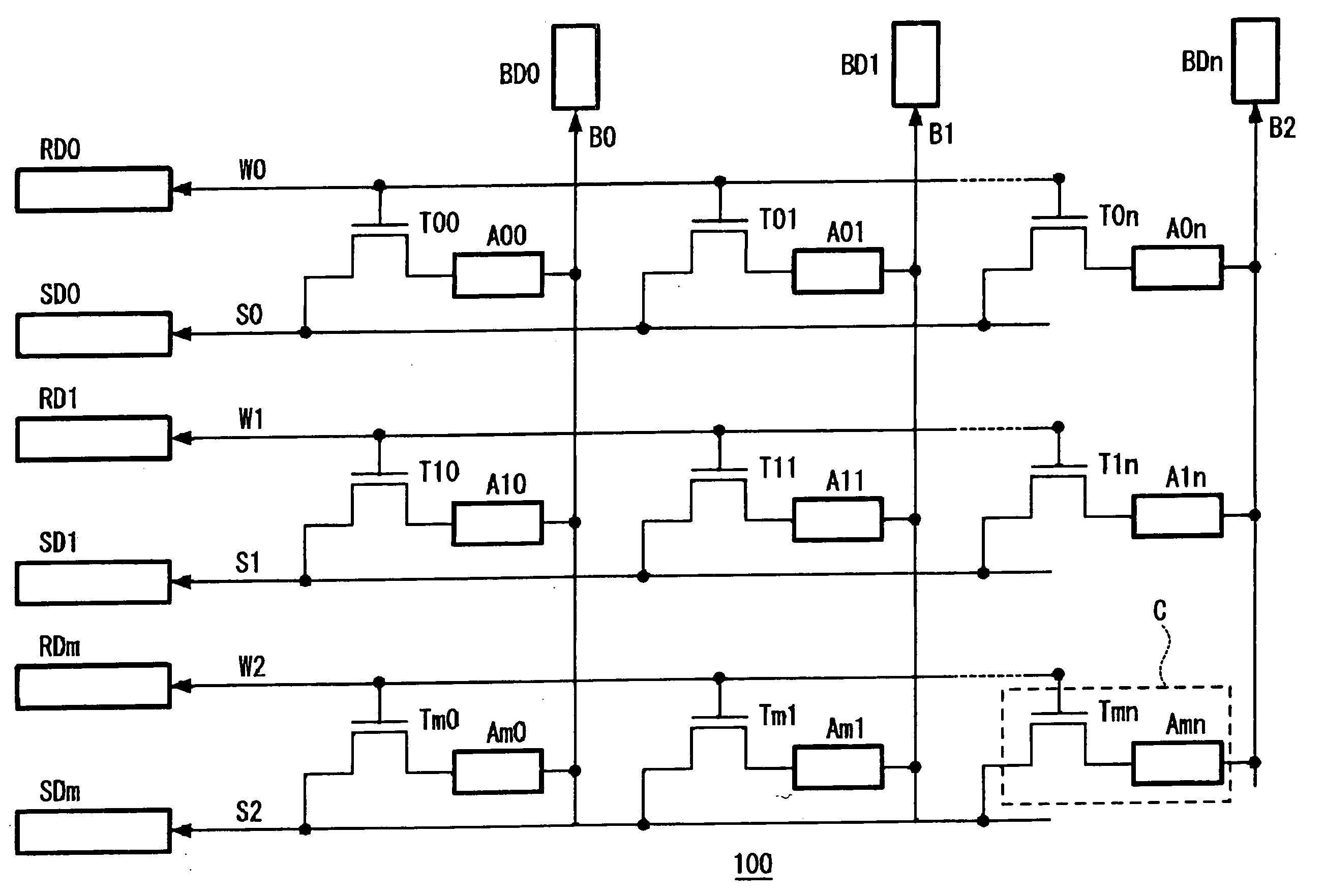
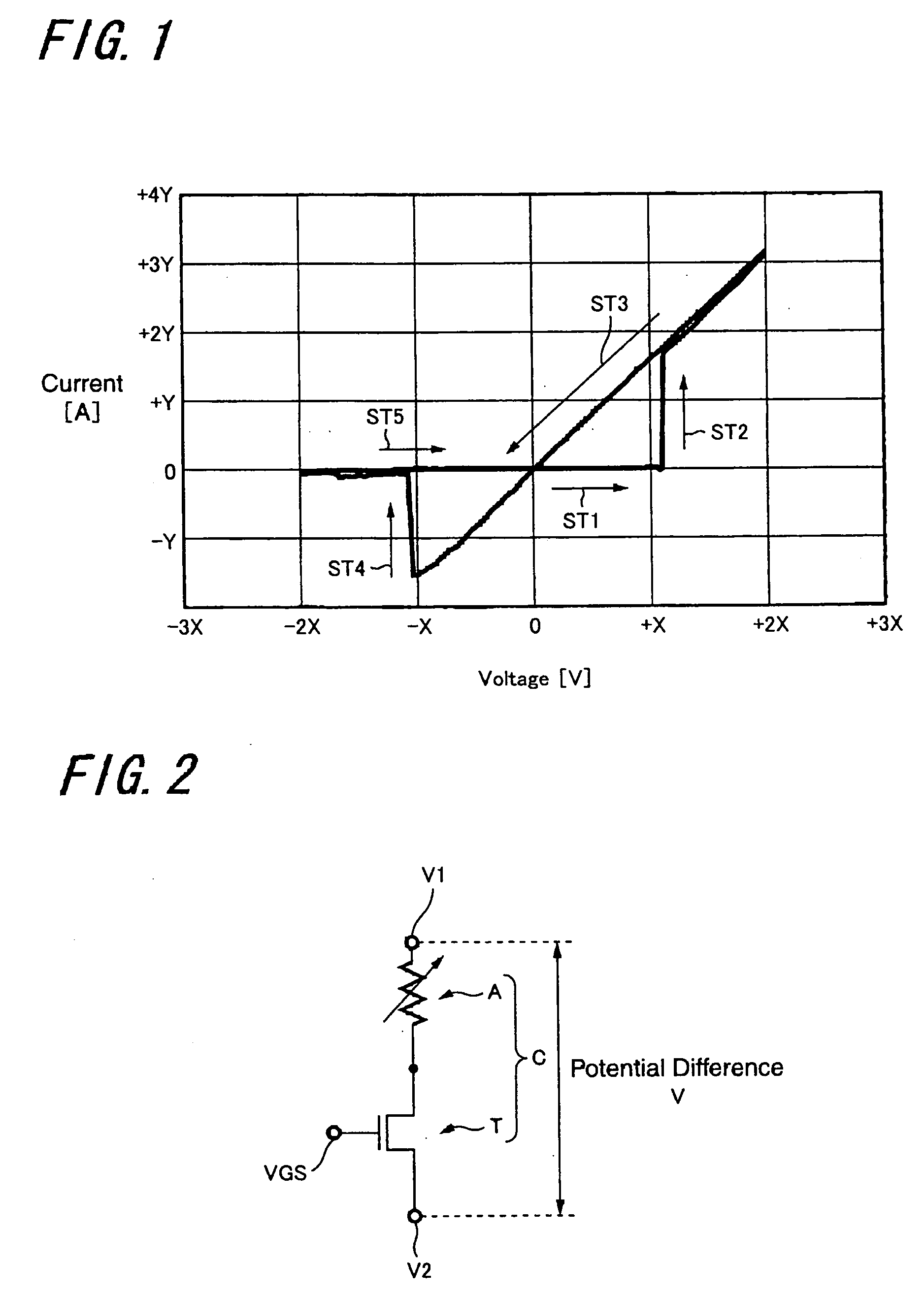
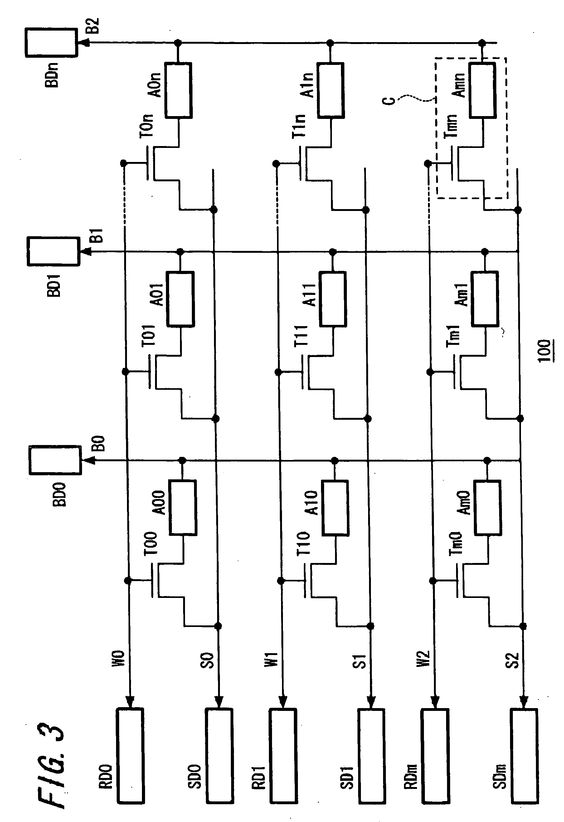
[0045] Hereinafter, an embodiment of a memory device according to the present invention is explained. In the present invention, a resistance change type memory element is used as a memory cell constituting the memory device.

[0046] First, FIG. 1 shows a voltage-current change of the resistance change type memory element which is used in the memory device of an embodiment of the memory device according to the present invention.

[0047] Specifically, this resistance change type memory element is in a state where current can not flow easily because a resistance value in an initial state is large (ST1); however, when a voltage equal to or more than a writing threshold voltage (+1.1X [V] of FIG. 1, several hundreds mV, for example) is applied, the current flows and the resistance value falls (ST2).

[0048] Then, the memory element changes to have an Ohmic characteristic (ST3) and enters a state where the current flows in proportion to the voltage.

[0049] After that, even if the voltage is ...


PUM


Abstract

A memory device is provided in which recording of multi-valued data can be performed at a high speed and the recording of multi-valued data can be performed with a drive circuit having comparatively simple configuration.
The memory device is formed of a memory cell including a memory element which stores information according to a state of electric resistance and a MIS transistor as a load connected in series to the memory element; and when an operation to change the memory cell from a state of high resistance value to a state of low resistance value is defined as writing and when an operation to change the memory cell from the state of low resistance value to the state of high resistance value is defined as erasing respectively, a resistance value of the memory element after writing is set to a plurality of different levels by controlling gate voltages VG1, VG2 and VG3, or the like, which are applied to the MIS transistor at the time of writing, so that different information is respectively assigned to each of the plurality of levels and to the state of high resistance value after erasing to store information of three values or more respectively into a memory element of each memory cell.

Description

BACKGROUND OF THE INVENTION [0001] 1. Field of the Invention [0002] The present invention relates to a memory device in which a memory cell is formed using a memory element which stores information according to a state of electric resistance. [0003] 2. Description of the Related Art [0004] Since a semiconductor nonvolatile memory such as a flash memory is small-sized and recorded data is maintained even after a power supply is turned off, it is widely used as a medium for recording a moving picture and audio. [0005] With respect to a nonvolatile memory, further greater recording capacity and recording density have been in demand. [0006] A nonvolatile memory having a structure capable of multi-value recording, specifically which can store data of 2 bits or more in one memory cell, has been proposed as a structure to obtain the above. [0007] At this time, in a case where the data of 2 bits can be recorded, for example, a memory element constituting a memory cell can maintain four kind...

Claims


Application Information

Patent Timeline
IPC IPC(8): G11C11/15G11C8/00G11C11/56G11C13/02G11C16/02G11C16/04G11C16/10
CPCG11C11/5614G11C11/5685G11C13/0007G11C13/0011G11C2213/79G11C13/0097G11C2013/0071G11C2213/32G11C2213/34G11C13/0069E03F5/0401E03F5/06E03F2005/066
Inventor TSUSHIMA, TOMOHITOARATANI, KATSUHISAKOUCHIYAMA, AKIRA
Owner SONY CORP
Why Eureka
Try Eureka