
Novel deposition method for si-ge epi layer on different intermediate substrates

a technology of sige epi layer and intermediate substrate, which is applied in the direction of basic electric elements, electrical apparatus, semiconductor devices, etc., to achieve the effect of increasing nucleation sites

Active Publication Date: 2005-08-11
TAIWAN SEMICON MFG CO LTD
View PDF6 Cites 8 Cited by
  • Summary
  • Abstract
  • Description
  • Claims
  • Application Information

AI Technical Summary

Benefits of technology

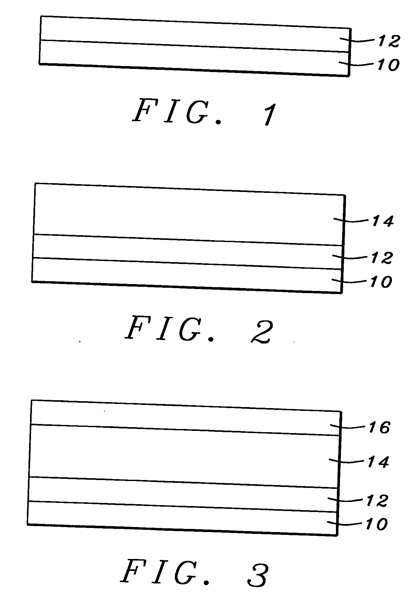
[0009] It has now been discovered that the above and other objects of the present invention may be accomplished in the following manner. Specifically, a structure is provided and a doped Si—Ge seed layer is formed thereover. The doped Si—Ge seed layer having increased nucleation sites. A Si—Ge epitaxial layer upon the doped Si—Ge seed layer whereby the Si—Ge epitaxial layer lacks discontinuity.

Problems solved by technology

However, the discontinuity of the Si—Ge epi layer occurs on different intermediate layers and becomes a major issue for subsequent process steps due to poor polysilicon (poly) sheet resistance connected with the base electrode.

Method used


Image

  • Novel deposition method for si-ge epi layer on different intermediate substrates
  • Novel deposition method for si-ge epi layer on different intermediate substrates

Examples


Embodiment Construction

Initial Structure—FIG. 1

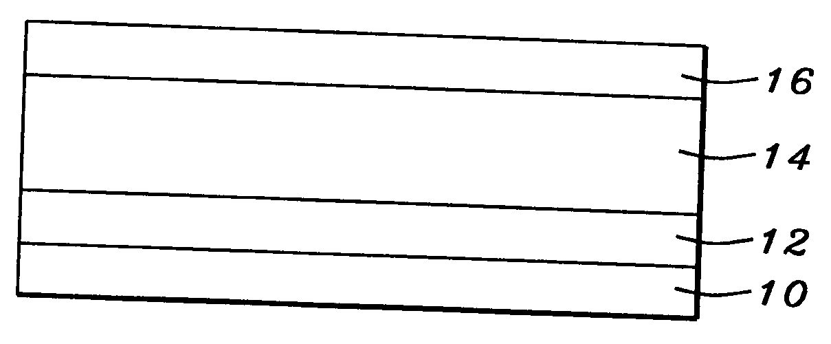
[0012] As shown in FIG. 1, structure 10 has a seed layer 12 formed thereover. Structure 10 is preferably an intermediate substrate and may be a silicon substrate and is understood to possibly include a semiconductor wafer or substrate, active and passive devices formed within the wafer, conductive layers and dielectric layers (e.g., inter-poly oxide (IPO), intermetal dielectric (IMD), etc.) formed over the wafer surface. The term “semiconductor structure” is meant to include devices formed within a semiconductor wafer and the layers overlying the wafer. Structure 10 may also include silicon oxide and / or polysilicon.

[0013] Seed layer 12 is preferably a doped Si—Ge layer having a thickness of preferably from about 10 to 400 Å and more preferably from about 20 to 200 Å. Doped Si—Ge seed layer 12 is preferably doped with boron (B), C, P or As and is more preferably doped with boron (B).

[0014] When doping with boron, B2H6 is introduced during the formation of S...


PUM


Abstract

A method of forming an Si—Ge epitaxial layer comprising the following steps. A structure is provided and a doped Si—Ge seed layer is formed thereover. The doped Si—Ge seed layer having increased nucleation sites. A Si—Ge epitaxial layer upon the doped Si—Ge seed layer whereby the Si—Ge epitaxial layer lacks discontinuity.

Description

BACKGROUND OF THE INVENTION [0001] Silicon-germanium epitaxial (Si—Ge epi) technology is becoming the mainstream in the application of heterojunction bipolar transistors. Si—Ge epi layers are used as the base material in such transistors in BiCMOS applications where bi-polar (BI) and complementary metal-oxide semiconductor (CMOS) transistors are fabricated in different areas of the same wafer. The Si—Ge epi layer could provide higher emitter injection efficiency and lower base transit time. [0002] However, the discontinuity of the Si—Ge epi layer occurs on different intermediate layers and becomes a major issue for subsequent process steps due to poor polysilicon (poly) sheet resistance connected with the base electrode. [0003] U.S. Pat. No. 6,388,307 B1 to Kondo et al. describes a B-doped SiGe layer in a transistor process. [0004] U.S. Pat. No. 5,976,941 to Boles et al. describes a SiGe epi process. [0005] U.S. Pat. No. 5,273,930 to Steele et al. describes a SiGe epi process on a s...

Claims


Application Information

Patent Timeline
Patent Type & Authority Applications(United States)
IPC IPC(8): H01L21/28H01L21/3205H01L21/331
CPCH01L21/02532H01L21/02579Y10S438/918H01L29/66242H01L21/0262
Inventor YAO, LIANG-GILEE, KUEN-CHYRCHEN, SHIH-CHANGLIANG, MONG-SONG
Owner TAIWAN SEMICON MFG CO LTD
Learn More