Nitride based semiconductor light-emitting device

a technology of semiconductor light-emitting devices and nitride, which is applied in semiconductor devices, electrical devices, packaging, etc., can solve problems such as the problem of obtaining a high luminous efficiency, and achieve the effects of preventing current loss, enhancing hole injection efficiency, and increasing hole mobility

Inactive Publication Date: 2005-08-18
SAMSUNG ELECTRO MECHANICS CO LTD
View PDF3 Cites 26 Cited by
  • Summary
  • Abstract
  • Description
  • Claims
  • Application Information

AI Technical Summary

Benefits of technology

[0013] Therefore, the present invention has been made in view of the above problems, and it is an object of the present invention to provide a nitride-based semiconductor light-emitting device which employs a p-type clad layer structure consisting of an electron blocking layer (EBL), an active layer and a layer for enhancing hole injection efficiency (hereinafter referred to as a “hole injection efficiency-enhancing layer”) interposed therebetween, thereby preventing electrons from overflowing and enhancing hole injection efficiency.
[0020] In order to enhance the injection efficiency of holes generated from the p-type clad layer while preventing current loss due to electron overflow, the p-type clad layer includes an electron blocking layer (EBL) as a nitride semiconductor layer containing Al, an active layer as a nitride semiconductor layer containing Al, and a nitride semiconductor layer containing no Al interposed between the two layers. The nitride semiconductor layer containing no Al, such as GaN, has a higher hole mobility (about 15 cm2 / Vs to about 20 cm2 / Vs) than the EBL containing Al (about 5 cm2 / Vs to about 10 cm2 / Vs). Further, from the viewpoint of hole concentration, a p-type GaN layer has a higher hole concentration (5×10¹⁷ / cm3) than a p-type AlGaN layer (about 1×10¹⁷ / cm3).
[0021] In conclusion, since the nitride semiconductor layer containing no Al, such as GaN, is interposed between the EBL and the active layer, electron overflow is prevented by the EBL containing Al. At the same time, since the nitride semiconductor layer containing no Al is placed in contact with the active layer, hole injection efficiency is markedly enhanced.

Problems solved by technology

However, since AlGaN not only has a lower hole mobility than any other nitride semiconductor layers, but also has a relatively low hole concentration (about 1×10¹⁷ / cm3), the injection efficiency of holes generated from the p-side electrode 19b to the active layer 15 may be lowered, thus causing a problem in obtaining a high luminous efficiency.

Method used


Image

  • Nitride based semiconductor light-emitting device
  • Nitride based semiconductor light-emitting device
  • Nitride based semiconductor light-emitting device

Examples


example 1

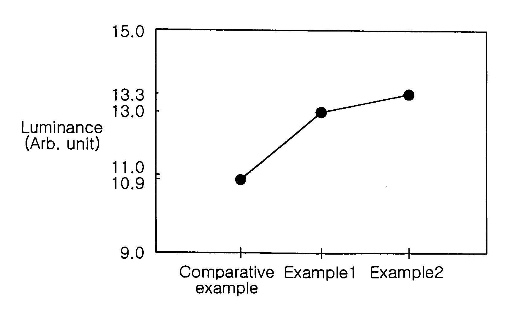
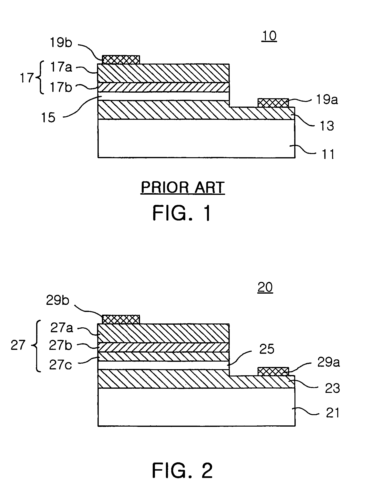
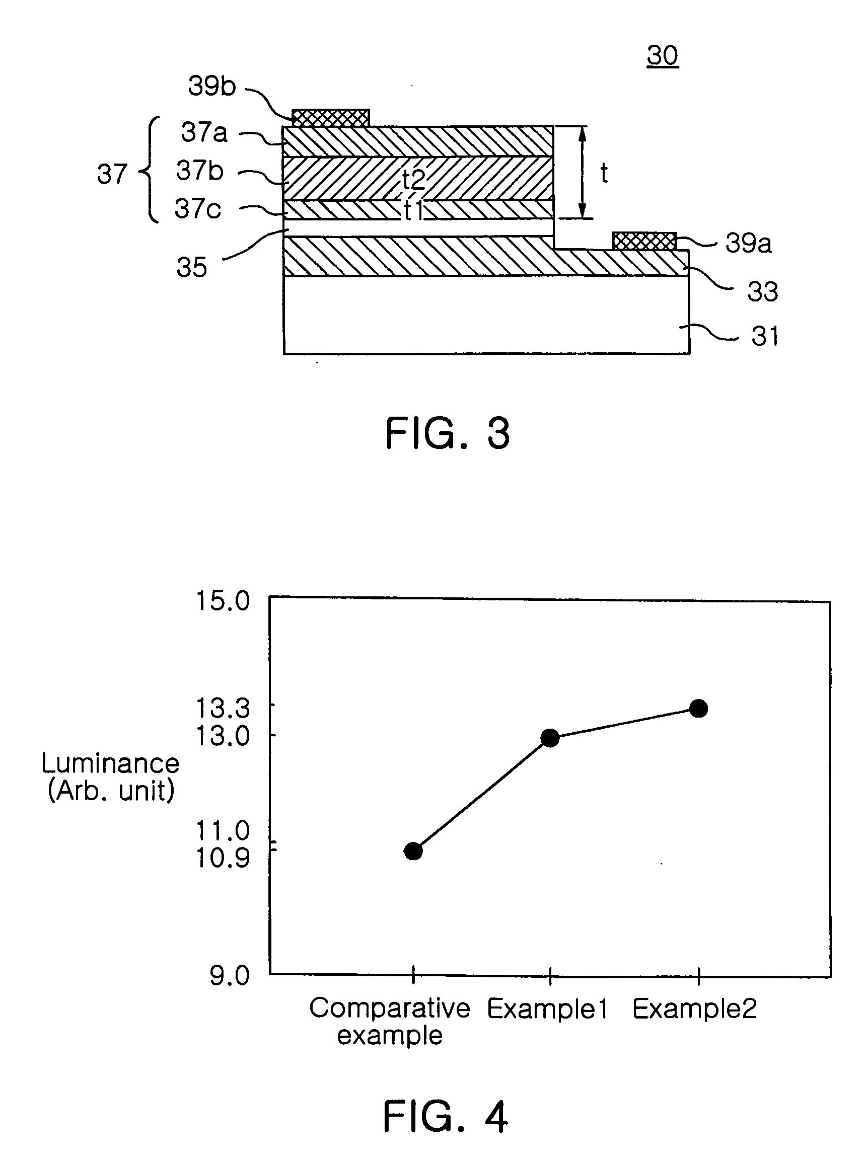
[0045] In order to identify the improvement in the characteristics of the nitride-based semiconductor light-emitting device according to the present invention, the nitride-based semiconductor light-emitting device shown in FIG. 2 was fabricated.

[0046] First, after a GaN low temperature-nuclei growing layer as a buffer layer was formed on a sapphire substrate, an n-type GaN clad layer was formed thereon so as to have an impurity concentration of 4×10¹⁸ / cm3. Thereafter, a multiple quantum well-structured active layer composed of five In0.15Ga0.85N quantum well layers and five GaN quantum barrier layers was formed on the n-type clad layer.

[0047] Further, a hole injection efficiency-enhancing layer made of p-type GaN, an electron blocking layer (EBL) made of p-type Al0.15Ga0.85N, and a contact layer made of p-type GaN were deposited sequentially on the active layer to prepare a p-type clad layer. The hole injection efficiency-enhancing layer was formed so as to have an impurity concen...

example 2

[0049] To observe changes in the characteristics of the nitride-based semiconductor light-emitting device of the present invention according to increasing thickness of the p-type EBL, the thickness of the EBL was increased, compared to in the light-emitting device fabricated in Example 1.

[0050] In this example, a nitride-based semiconductor light-emitting device was fabricated in the same manner as in Example 1, except that the structure of the p-type clad layer was varied. Specifically, a hole injection efficiency-enhancing layer was made of p-type GaN so as to have an impurity concentration of about 5×10¹⁷ / cm3 and a thickness of about 20 nm, an electron blocking layer was made of p-type Al0.15Ga0.85N so as to have an impurity concentration of 1×10¹⁷ / cm3 and a thickness of about 69 nm, and a p-type contact layer was made of p-type GaN so as to have an impurity concentration of 5×10¹⁷ / cm3 and a thickness of about 76 nm.


PUM


Abstract

Disclosed herein is a nitride-based semiconductor light-emitting device. The nitride-based semiconductor light-emitting device comprises an n-type clad layer made of n-type Alx1Iny1Ga(1−x1−y1)N (where 0≦x1≦1, 0≦y1≦1, and 0≦x1+y1≦1), a multiple quantum well-structured active layer made of undoped InAGa1−AN (where 0<A<1) formed on the n-type clad layer, and a p-type clad layer formed on the active layer wherein the p-type clad layer includes at least a first layer made of p-type Iny2Ga1−y2N (where 0≦y2<1) formed on the active layer and a second layer made of p-type Alx3Iny3Ga(1−x3−y3)N (where 0<x3≦1, 0≦y3≦1, and 0<x3+y3≦1) formed on the first layer.

Description

BACKGROUND OF THE INVENTION [0001] 1. Field of the Invention [0002] The present invention relates to a nitride-based semiconductor light-emitting device, and more particularly to a nitride-based semiconductor light-emitting device which employs a p-type clad layer structure with enhanced hole injection efficiency into an active layer, thereby exhibiting a high luminous efficiency. [0003] 2. Description of the Related Art [0004] Generally, nitride-based semiconductor light-emitting devices are optical devices with a high output that generate short-wavelength light in the blue and green ranges and the like, and thus enable realization of the full color spectrum. For these reasons, nitride-based semiconductor light-emitting devices have drawn attention in related industrial fields. [0005] Nitride-based semiconductor light-emitting devices are semiconductor single crystals composed of AlxInyGa(1−x−y)N (wherein 0≦x≦y, 0≦y≦1 and 0≦x+y≦1) which can be grown on substrates, e.g., sapphire an...

Claims


Application Information

Patent Timeline
Patent Type & Authority Applications(United States)
IPC IPC(8): H01L29/06H01L33/06H01L33/32
CPCB82Y20/00H01L33/04H01L33/32H01L33/06A23L5/13A23L17/60B65B7/00B65B25/06
Inventor KIM, JE WONOH, JEONG TAKKIM, DONG JOONKIM, SUN WOONPARK, JIN SUBLEE, KYU HAN
Owner SAMSUNG ELECTRO MECHANICS CO LTD
Why Eureka
Try Eureka