Chip multiprocessor for media applications

a multi-processor and media technology, applied in the field of data processing systems, can solve the problems of cpus performance increase, lack of scalability of multi-issue uni-processor architecture, and soon reaching the point of diminishing returns, and scaling problems began to appear

US20050182915A1Inactive Publication Date: 2005-08-18DEVANEY PATRICK +2
9 Cites 15 Cited by

Patent Information

Authority / Receiving Office
US · United States
Current Assignee / Owner
Publication Date
2005-08-18
Estimated Expiration
Not applicable · inactive patent

Smart Images

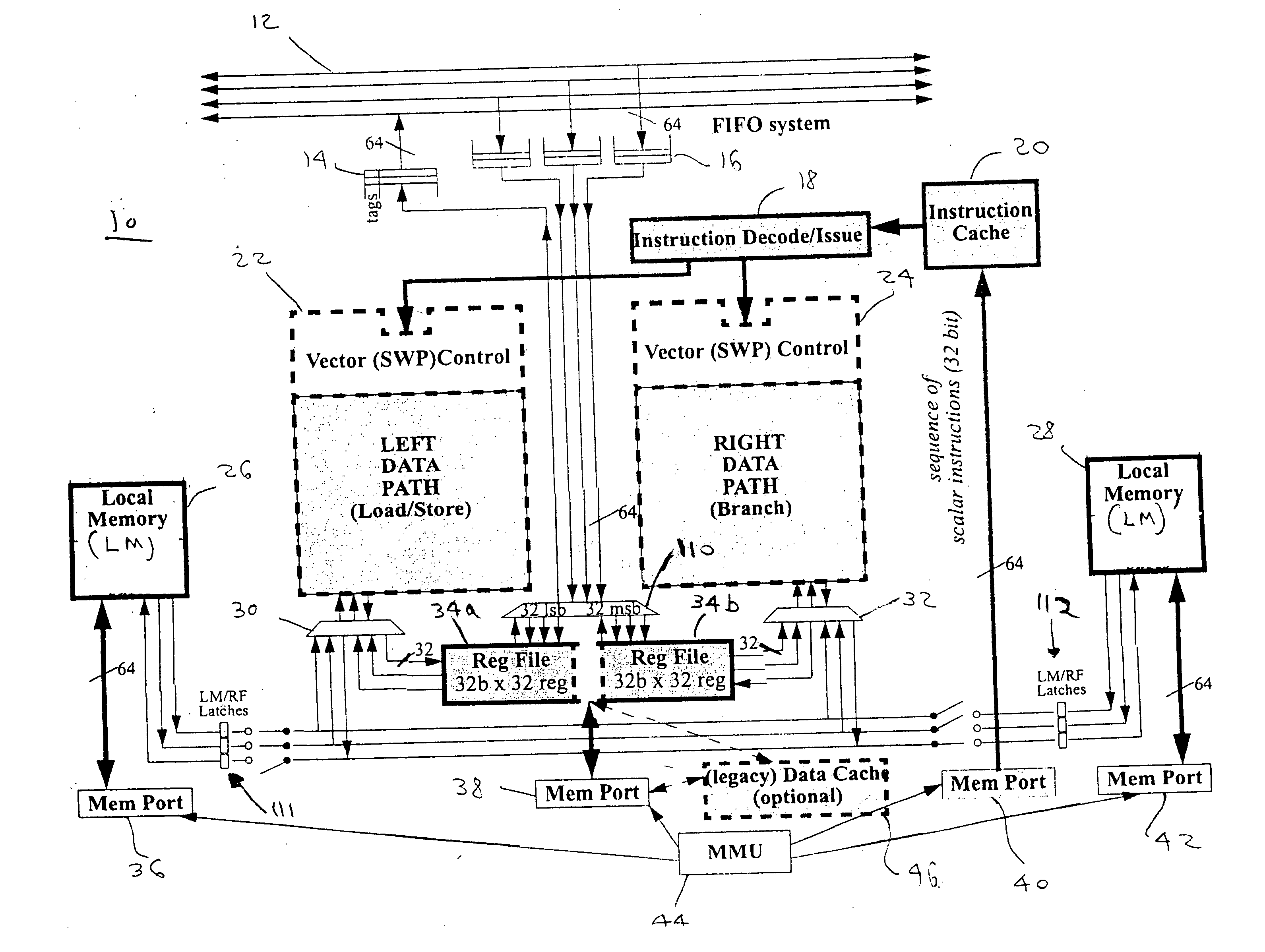
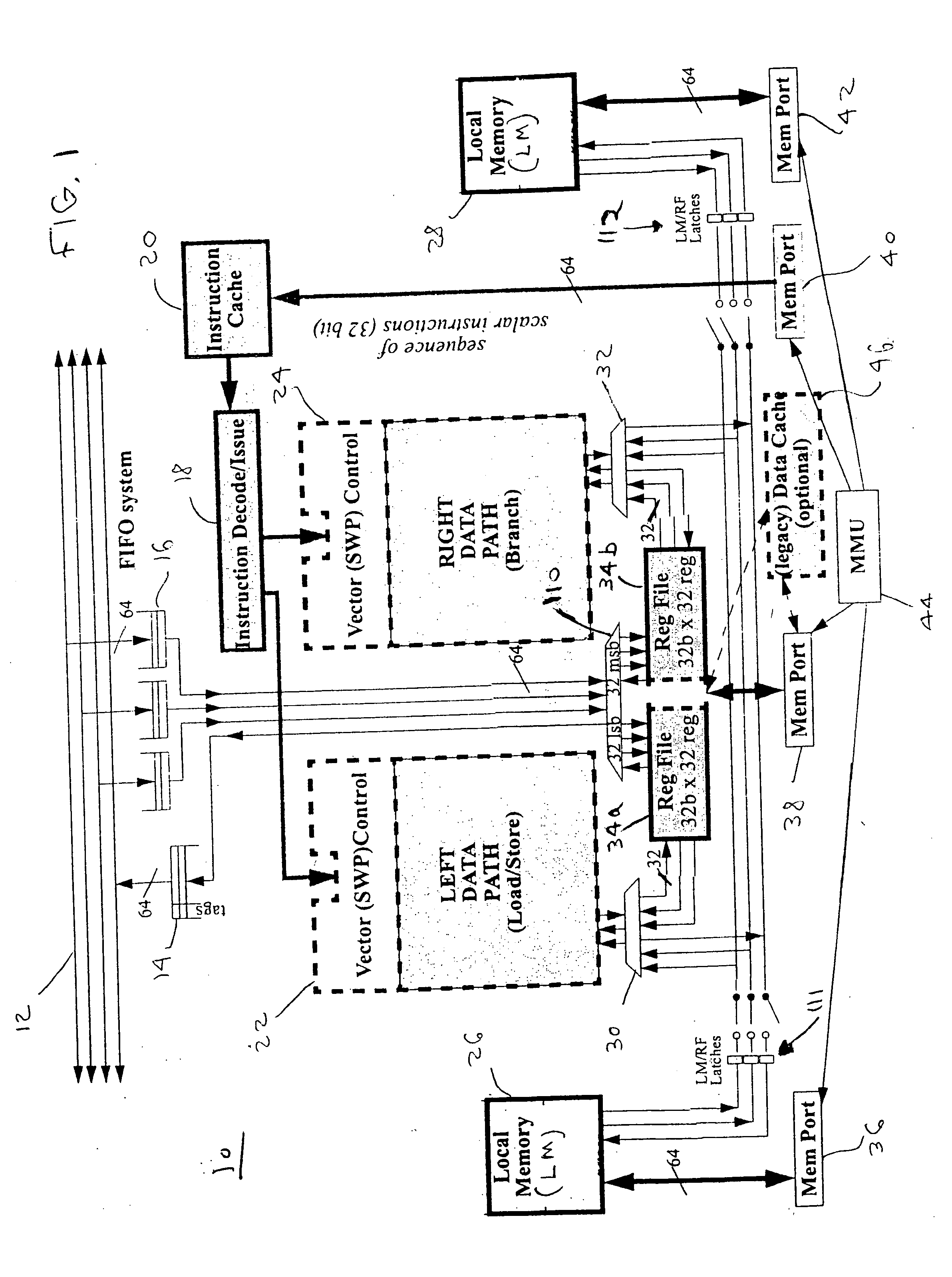
  • Figure 1
    Figure 1
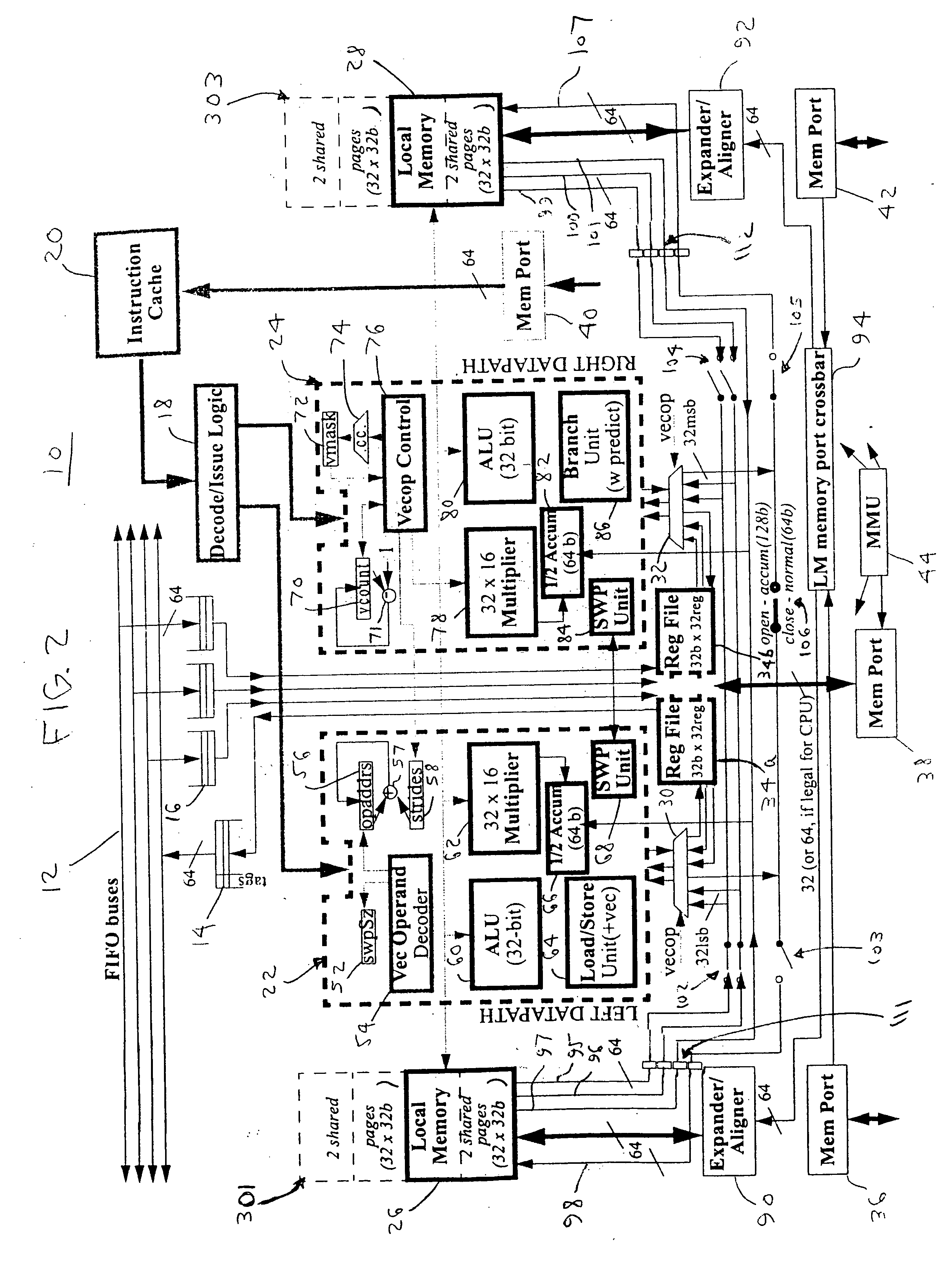
  • Figure 2
    Figure 2
  • Figure 3
    Figure 3
Patent Text Reader

Abstract

A chip multiprocessor (CMP) includes a plurality of processors disposed on a peripheral region of a chip. Each processor has (a) a dual datapath for executing instructions, (b) a compiler controlled register file (RF), coupled to the dual datapath, for loading / storing operands of an instruction, and (c) a compiler controlled local memory (LM), a portion of the LM disposed to a left of the dual datapath and another portion of the LM disposed to a right of the dual datapath, for loading / storing operands of an instruction. The CMP also has a shared main memory disposed at a central region of the chip, a crossbar system for coupling the shared main memory to each of the processors, and a first-in-first-out (FIFO) system for transferring operands of an instruction among multiple processors.
Need to check novelty before this filing date? Find Prior Art

Description

TECHNICAL FIELD

[0001] The present invention relates, in general, to data processing systems and, more specifically, to a homogeneous chip multiprocessor (CMP) built from clusters of multiple central processing units (CPUs). BACKGROUND OF THE INVENTION

[0002] Advances in semiconductor technology have created reasonably-priced chips with literally hundreds of millions of transistors. This transistor budget has revealed the lack of scalability of both multi-issue uni-processor architectures, such as instruction level parallelism (ILP) (superscalar and VLIW), and of the classic vector architecture. The most common use for the increased transistor budget in CPU designs has been to increase the amount of on-chip cache. The performance increase in such CPUs, however, soon reached the point of diminishing returns.

[0003] As semiconductor design rules shrank, some scaling problems began to appear. Wire delays have failed to scale. This issue has been postponed for about one silicon process ...

Examples

Embodiment Construction

[0025] Referring to FIG. 1, there is shown a block diagram of a central processing unit (CPU), generally designated as 10. CPU 10 is a two-issue-super-scalar (2i-SS) instruction processor-core capable of executing multiple scalar instructions simultaneously or executing one vector instruction. A left data path processor, generally designated as 22, and a right data path processor, generally designated as 24, receive scalar or vector instructions from instruction decoder 18.

[0026] Instruction cache 20 stores read-out instructions, received from memory port 40 (accessing main memory), and provides them to instruction decoder 18. The instructions are decoded by decoder 18, which generates signals for the execution of each instruction, for example signals for controlling sub-word parallelism (SWP) within processors 22 and 24 and signals for transferring the contents of fields of the instruction to other circuits within these processors.

[0027] CPU 10 includes an internal register file ...