NAND flash controller and data exchange method between NAND flash memory and NAND flash controller

Active Publication Date: 2009-04-09
ROCKCHIP ELECTRONICS CO LTD
View PDF11 Cites 67 Cited by
  • Summary
  • Abstract
  • Description
  • Claims
  • Application Information

AI Technical Summary

Benefits of technology

[0011]An object of the present invention is to provide a NAND flash controller which is able to

Problems solved by technology

However, the command conversion information which may be stored in the command data decoder 13 is finite and it is difficult to include all of the command conversion information in connection with all manufacturers.
Moreover, because the NAND flash memory develops rapidly, the solution in which the comman

Method used


Image

  • NAND flash controller and data exchange method between NAND flash memory and NAND flash controller
  • NAND flash controller and data exchange method between NAND flash memory and NAND flash controller
  • NAND flash controller and data exchange method between NAND flash memory and NAND flash controller

Examples


first embodiment

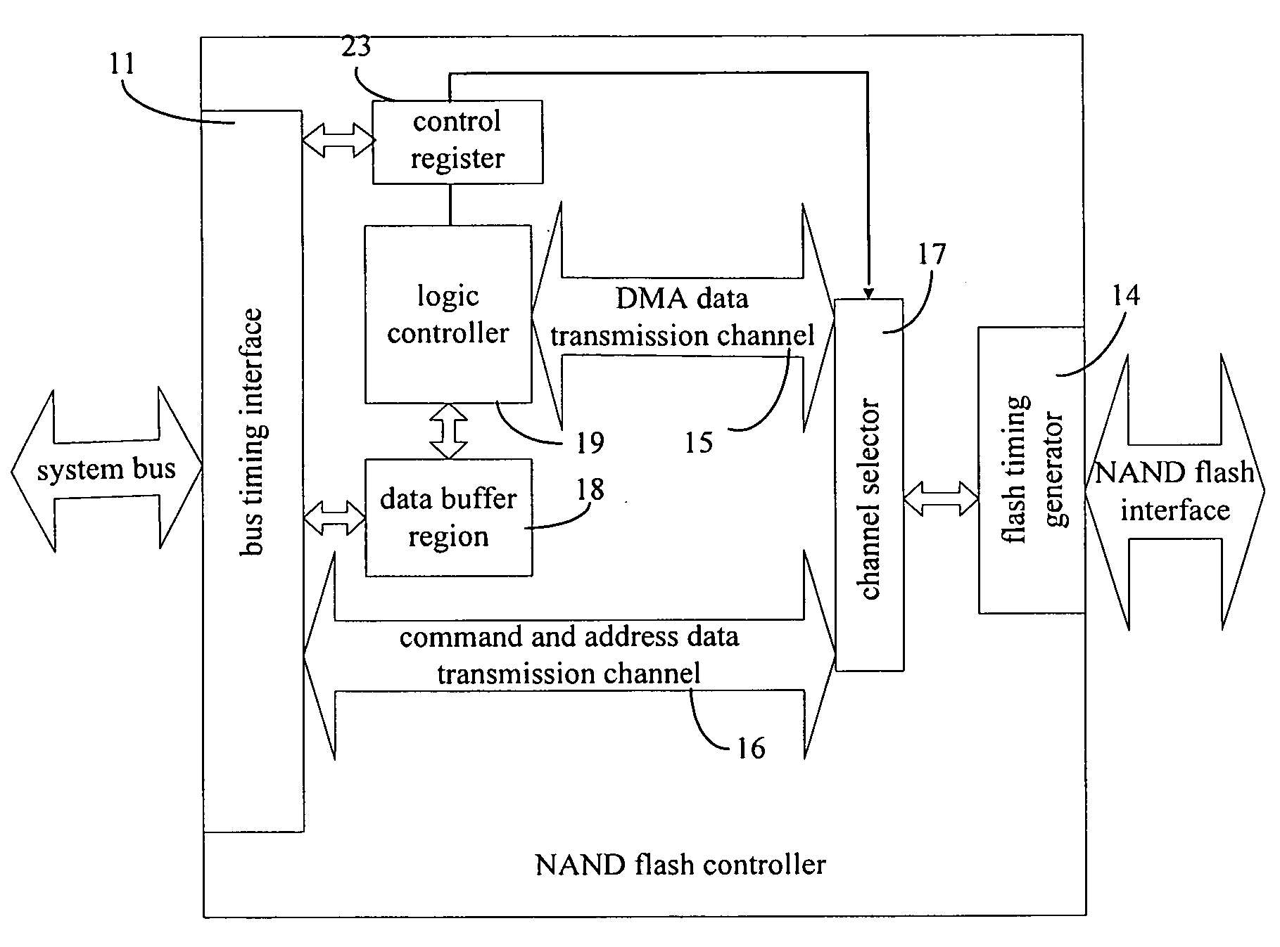
[0050]FIG. 2 is a schematic diagram showing the NAND flash controller according to the present invention. As shown in FIG. 2, the NAND flash controller includes a bus timing interface 11, a FLASH timing generator 14, a DMA data transmission channel 15, a command and address data transmission channel 16, a channel selector 17, a data buffer region 18, a logic controller 19 and a control register 23.

[0051]The bus timing interface 11 is connected with the system bus for implementing the data exchange. The data includes message data and command and address data. The bus timing interface 11 writes the command and address date transmitted on the system bus into the NAND flash memory through the command and address data transmission channel 16, the channel selector 17 and the FLASH timing generator 14. The message data is written into the data buffer region 18 through the bus timing interface 11.

[0052]The command and address data transmission channel 16 connects the bus timing interface 11...

second embodiment

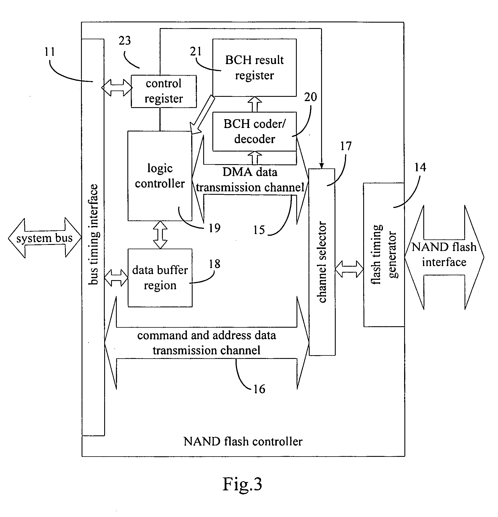
[0059]FIG. 3 is a schematic diagram showing the NAND flash controller according to the present invention. The NAND flash controller includes a bus timing interface 11, a flash timing generator 14, a DMA data transmission channel 15, a command and address data transmission channel 16, a channel selector 17, a data buffer region 18, a logic controller 19, a BCH coder / decoder 20, a BCH result register 21 and a control register 23.

[0060]When the message data is to be written into the NAND flash memory, the BCH coder / decoder 20 performs the coding to the message data and stores the coding result in the BCH result register 21. The logic controller 19 reads the coding result from the BCH result register 21 and writes corresponding check bit into the NAND flash memory through the DMA data transmission channel 15.

[0061]When the message data is to be read out from the NAND flash memory, the BCH coder / decoder 20 performs the decoding to the message data and stores the decoding result in the BC...

third embodiment

[0066]FIG. 4 is a schematic diagram showing the NAND flash controller according to the present invention. The NAND flash controller includes a bus timing interface 11, a flash timing generator 14, a DMA data transmission channel 15, a command and address data transmission channel 16, a channel selector 17, a data buffer region 18, a logic controller 19, a BCH coder / decoder 20, a BCH result register 21, a flash timing control register 22 and a control register 23.

[0067]The flash timing control register 22 takes the period of the system bus clock HCLK as the time unit to store time values such as the establishment time of the chip selection enable signal, the effective width of the writing / reading signal, the holding time of the chip selection enable signal, the establishment time of the command / address signal and the holding time of the command / address signal.

[0068]Because the time values in different NAND flash memories are different, the NAND flash controller sets the time values f...


PUM


Abstract

The invention discloses a NAND flash controller, including a command and address data transmission channel adapted to connect the bus timing interface with the channel selector and transmit command and address data, a data buffer region adapted to receive message data from the bus timing interface through system bus, a control register adapted to receive an operation parameter configured through system bus via the bus timing interface, a logic controller adapted to write the data information into or read the data information from the data buffer region according to the operation parameter, a channel selector adapted to connect the DMA data transmission channel or the command and address data transmission channel according to the operation parameter for transmitting data. The invention also discloses a date exchange method between NAND flash controller and NAND flash memory. The invention improves the data transmission efficiency and is compatible with various NAND flash memories.

Description

FIELD OF THE INVENTION [0001]The present invention relates to the field of NAND flash controller, and in particular, to a NAND flash controller and a date exchange method between the NAND flash controller and a NAND flash memory.BACKGROUND OF THE INVENTION [0002]The NAND flash memory is a nonvolatile semiconductor memory which can be electrically erased and written online. The NAND flash memory has many advantages, such as high erasing and writing speed, low power consumption, large capacity and low cost. The NAND flash memory may be applied in many electronic products, such as MP3, MP4, cell phone, digital camera and video camera. The data is written into or read from the NAND flash memory via the NAND flash controller. The data transmitted to the NAND flash memory includes address and command data and message data. In the prior art, the address and command data and message data are sent to the NAND flash memory via an internal data transmission channel.[0003]FIG. 1 is a structure ...

Claims


Application Information

Patent Timeline
IPC IPC(8): G06F12/02
CPCG11C7/22G06F13/385
Inventor QUE, JINZHEN
Owner ROCKCHIP ELECTRONICS CO LTD
Why Eureka
Try Eureka